1
PS8634C 09/13/04
Features
∑ CMOS Technology for Bus and Analog Applications
∑ Low On-Resistance: 2 at 3.0V
∑ Wide V
CC
Range: +1.8V to +5.5V
∑ Low Power Consumption : 5µW
∑ Rail-to-Rail switching throughout Signal Range
∑ Fast Switching Speed: 30ns max. at 5V
∑ High Off Isolation: ≠57dB at 10MHz
∑ ≠57dB (1 MHz) Crosstalk Rejection Reduces Signal Distortion
∑ Break-Before-Make Switching
∑ Extended Industrial Temperature Range: ≠40
∞
C to 85
∞
C
∑ Low On-Resistance Replacement for NC7SB3157
∑ Packaging (Pb-free & Green available):
- 6-pin SOT-23 (T)
- 6-contact TDFN-6 (ZC)
Applications
∑ Cell Phones
∑ PDAs
∑ Portable Instrumentation
∑ Battery Powered Communications
∑ Computer Peripherals
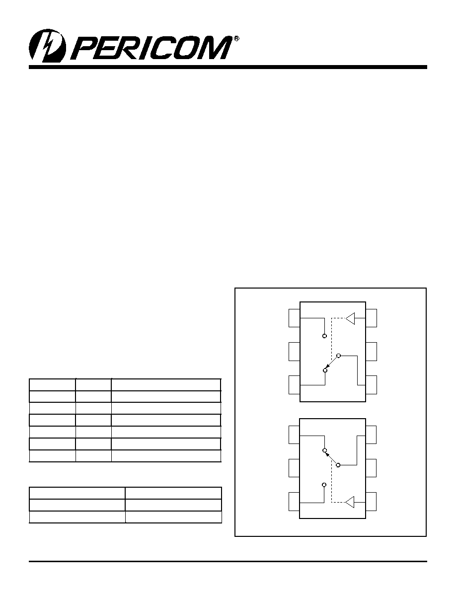
PI5A3159
SOT
INY
TM
1 Low-Voltage
SPDT Analog Switch
Description
The PI5A3159 is a high-bandwidth, fast single-pole double-throw
(SPDT) CMOS switch. It can be used as an analog switch or as
a low-delay bus switch. Specified over a wide operating power
supply voltage range, 1.8V to 5.5V, the PI5A3159 has a maximum
On-Resistance of 4 at 1.8V, 2.4 at 2.3V & 1 at 4.5V.
Break-before-make switching prevents both switches being
enabled simultaneously. This eliminates signal disruption during
switching.
Control input, S, tolerates input drive signals up to 5.5V, inde-
pendent of supply voltage.
PI5A3159 is a low On-Resistance replacement for the PI5A3157
and NC7SB3157.
Logic Function Table
Logic Input(s)
Function
0
B
0
Connected to A
1
B
1
Connected to A
Connection Diagrams
B
1
GND
1
2
3
6
4
B
0
S
5 V
CC
A
B
0
GND
1
2
3
6
4
B
1
A
5 V
CC
S
SOT-23
TDFN
Pin Description
Pin Number Name
Description
1
B
1
Data Port
2
GND
Ground
3
B
0
Data Port (Normally Closed)
4
A
Common Output/Data Port
5
V
CC
Positive Power Supply
6
S
Logic Control
2
PS8634C 09/13/04
PI5A3159
SOT
INY
TM
1 Low-Voltage
SPDT Analog Switch
Caution: Stresses beyond those listed under "Absolute Maximum Ratings" may cause permanent damage to the device. This is a
stress only rating and operation of the device at these or any other conditions beyond those indicated in the operational sections of
this specification is not implied.
Absolute Maximum Ratings
Voltages Referenced to GND
V+ ...................................................................... ≠0.5V to +5.5V
V
IN
, V
COM
, V
NC
, V
NO
(1)
............................≠0.5V to V
+
+0.3V
or 30mA, whichever occurs first
Current (any terminal)................................................... ±200mA
Peak Current, COM, NO, NC
(Pulsed at 1ms, 10% duty cycle)................................... ±400mA
Note:
1. Signals on NC, NO, COM, or IN exceeding V+ or GND are clamped
by internal diodes. Limit forward diode current to 30mA.
Thermal Information
Continuous Power Dissipation
SOT23 (derate 7.1mW/∫C above +70∫C)............................ 0.5W
Storage Temperature ........................................≠65∫C to +150∫C
Lead Temperature (soldering, 10s) ................................. +300∫C
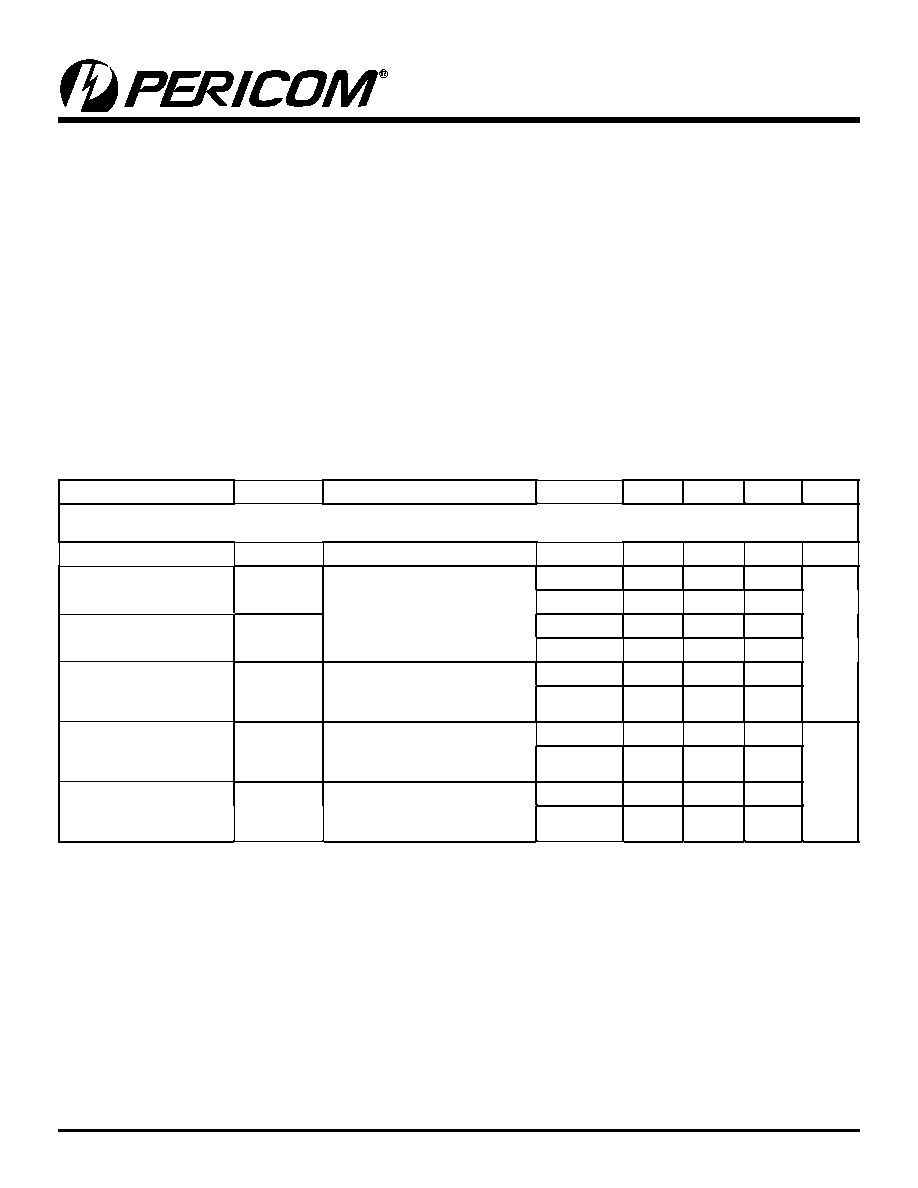
Electrical Specifications - Single +5V Supply
(V+ = +5V ± 10%, GND = 0V, V
INH
= 2.4V, V
INL
= 0.8V)
Parameter
Symbol
Conditions
Temp(∞C)
Min
(1)
Typ
(2)
Max
(1)
Units
Analog Switch
Analog Signal Range
(3, 4)
V
ANALOG
Full
0
V+
V
On-Resistance
R
ON
V+ = 4.5V,
I
COM
= -30mA,
V
NO
or V
NC
= +2.5V
25
0.70
0.90
Full
1.1
On-Resistance Match
Between Channels
(5)
R
ON
25
0.03
0.05
Full
0.10
On-Resistance Flatness
(6)
R
FLAT(ON)
V+ = 4.5V,
I
COM
= -30mA,
V
NO
or V
NC
= 1V, 1.5V, 2.5V
25
0.08
0.12
Full
0.15
NO or NC Off Leakage
Current
(7)
I
NO(OFF)
or
I
NC(OFF)
V+ = 5.5V,
V
COM
= 0V,
V
NO
or V
NC
= 4.5V
25
2
0.01
2
nA
Full
-20
20
COM On Leakage Cur-
rent
(7)
I
COM(ON)
V+ = 5.5V,
V
COM
= 4.5V,
V
NO
or V
NC
= 4.5V
25
-4
4
Full
-40
0.3
40
3
PS8634C 09/13/04
PI5A3159
SOT
INY
TM
1 Low-Voltage
SPDT Analog Switch
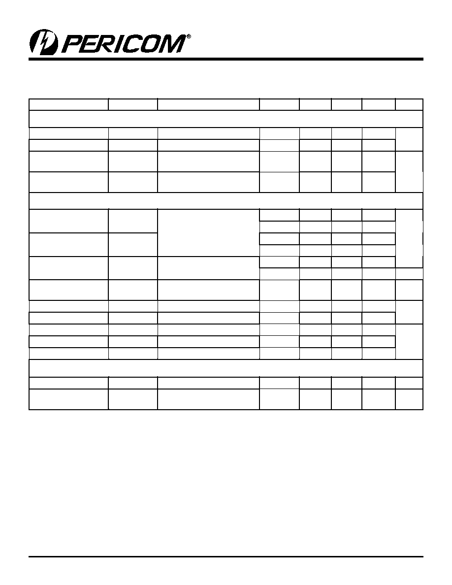
Electrical Specifications - Single +5V Supply
(continued)
(V+ = + 5V ± 10%, GND = 0V, V
INH
= 2.4V, V
INL
= 0.8V)
Parameter
Symbol
Conditions
Temp(∞C)
Min
(1)
Typ
(2)
Max
(1)
Units
Analog Switch
Input HIGH Voltage
V
IH
Guaranteed Logic HIGH level
V
Input LOW Voltage
V
IL
Guaranteed Logic LOW level
0.8
Input Current with
HIGH Voltage
I
INH
V
IN
= 2.4V, all others = 0.8V
-1
0.005
1
µA
Input Current with LOW
Voltage
I
INL
V
IN
= 0.8V, all others = 2.4V
-1
0.005
1
Dynamic
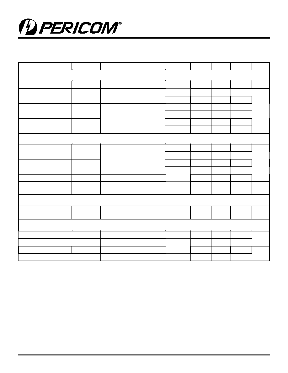
Turn-On-Time
t
ON
V
CC
= 5V,
See Fig. 1
25
20
35
ns
Full
40
Turn-Off-Time
t
OFF
25
15
20
Full
35
Break-Before-Make
t
BBM
See Fig. 3
25
1
12
14.5
Full
1
17.5
Charge Injection
(3)
Q
C
L
-1nF, V
GEN
= 0V,
R
GEN
= 0V, See Fig 2
25
40
pC
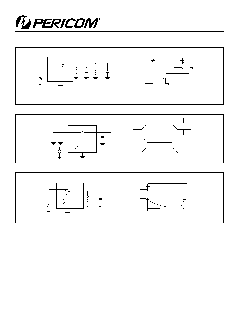
Off Isolation
O
IRR
R
L
= 50, f = 1MHz, See Fig 4
-57
dB
CrossTalk
(9)
X
TALK
R
L
= 50, f = 1MHz, See Fig 4
-57
NC or NO Capacitance
C
NC/NO(OFF)
f = 1MHz, See Fig 6
42
pF
COM Off Capacitance
C
COM(OFF)
f = 1MHz, See Fig 6
83
COM On Capacitance
C
COM(ON)
f = 1MHz, See Fig 7
130
Supply
Power-Supply Range
V+
Full
1.8
5.5
V
Positive Supply Current
1+
V+ = 5.5V, V
IN
= 0V or V+,
All Channels ON or OFF
Full
0.5
1
µA
Notes:
1. The algebraic convention, where most negative value is a minimum and most positive is a maximum, is used in this data sheet.
2. Typical values are for DESIGN AID ONLY, not guaranteed or subject to production testing.
3. Guaranteed by design.
4. Device is NOT guaranteed to function per the datasheet specification outside of 0 to V+ range.
5. R
ON
=
R
ON
max. - R
ON
min.
6. Flatness is defined as the difference between the maximum and minimum value of On-resistance measured.
7. Leakage parameters are 100% tested at maximum rated hot temperature and guaranteed by correlation at +25∫C.
8. Off Isolation = 20log
10
[ V
COM
/ (V
NO
or V
NC
)
]. See Figure 4.
9. Between any two switches. See Figure 5.

4
PS8634C 09/13/04
PI5A3159
SOT
INY
TM
1 Low-Voltage
SPDT Analog Switch
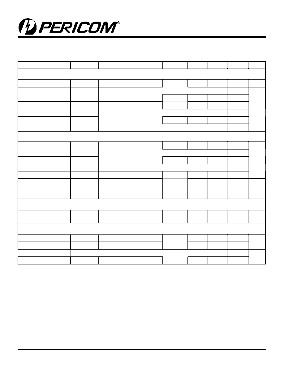
Electrical Specifications - Single +3.3V Supply
(V+ = +3.3V ± 10%, GND = 0V, V
INH
= 2.0V, V
INL
= 0.6V)
Parameter
Symbol
Conditions
Temp(∞C)
Min
(1)
Typ
(2)
Max
(1)
Units
Analog Switch
Analog Signal Range
(3)
V
ANALOG
0
V+
V
On-Resistance
R
ON
V+ = 3V, I
COM
= -24mA,
V
NO
or V
NC
= 2.0V
25
1.4
1.8
Full
2.2
On-Resistance Match
Between Channels
(4)
R
ON
V+ = 3.3V, I
COM
= -24mA,
V
NO
or V
NC
= 0.8V, 2.0V
25
0.04
0.05
Full
0.11
On-Resistance Flatness
R
FLAT(ON)
25
0.17
0.2
Full
0.25
Dynamic
Turn-On-Time
t
ON
V
CC
= 5V,
See Fig. 1
25
30
40
ns
Full
55
Turn-Off-Time
t
OFF
25
20
25
Full
40
Break-Before-Make
t
BBM
See Fig. 3
25
1
21
29
Charge Injection
(3)
Q
C
L
-1nF, V
GEN
= 0V,
R
GEN
= 0V, See Fig 2
25
30
pC
Supply
Positive Supply Current
1+
V+ = 3.6V, V
IN
= 0V or V+,
All Channels ON or OFF
Full
0.5
1
µA
Logic Input
Input HIGH Voltage
V
IH
Guaranteed Logic HIGH level
Full
2
V
Input LOW Voltage
V
IL
Guaranteed Logic LOW level
Full
0.6
Input HIGH Current
I
INH
V
IN
= 2.4V, all others = 0.8V
Full
-1
1
µA
Input LOW Current
I
INL
V
IN
= 0.8V, all others = 2.4V
Full
-1
1
Notes:
1. The algebraic convention, where most negative value is a minimum and most positive is a maximum, is used in this data sheet.
2. Typical values are for DESIGN AID ONLY, not guaranteed or subject to production testing.
3. Guaranteed by design.
4. R
ON
=
R
ON
max. - R
ON
min.
5. Flatness is defined as the difference between the maximum and minimum value of On-Resistance measured.
5
PS8634C 09/13/04
PI5A3159
SOT
INY
TM
1 Low-Voltage
SPDT Analog Switch
Electrical Specifications - Single +2.5V Supply
(V+ = +2.5V ± 10%, GND = 0V, V
INH
= 1.8V, V
INL
= 0.6V)
Parameter
Symbol
Conditions
Temp(∞C)
Min
(1)
Typ
(2)
Max
(1)
Units
Analog Switch
Analog Signal Range
(3)
V
ANALOG
0
V+
V
On-Resistance
R
ON
V+ = 1.8V, I
COM
= -2mA,
V
NO
or V
NC
= 1.5V
25
1.6
2
Full
2.7
On-Resistance Match
Between Channels
(4)
R
ON
V+ = 1.8V, I
COM
= -2mA,
V
NO
or V
NC
= 0.8V, 1.5V
25
0.13
0.16
Full
0.2
On-Resistance Flatness
R
FLAT(ON)
25
0.25
0.3
Full
0.45
Dynamic
Turn-On-Time
t
ON
V+ = 2.5V,
V
NO
or V
NC
= 1.8V,
See Fig. 1
25
40
55
ns
Full
70
Turn-Off-Time
t
OFF
25
30
40
Full
55
Break-Before-Make
t
BBM
See Fig. 3
25
1
33
39
Make-Before-Break
t
MBB
See Fig. 4
25
1
9
13
Charge Injection
(3)
Q
C
L
-1nF, V
GEN
= 0V,
R
GEN
= 0V, See Fig 2
25
20
pC
Supply
Positive Supply Current
1+
V+ = 2.75V, V
IN
= 0V or V+,
All Channels ON or OFF
Full
0.5
1
µA
Logic Input
Input HIGH Voltage
V
IH
Guaranteed Logic HIGH level
Full
1.8
V
Input LOW Voltage
V
IL
Guaranteed Logic LOW level
Full
0.6
Input HIGH Current
I
INH
V
IN
= 2.0V, all others = 0.8V
Full
-1
1
µA
Input LOW Current
I
INL
V
IN
= 0.8V, all others = 2.0V
Full
-1
1
Notes:
1. The algebraic convention, where most negative value is a minimum and most positive is a maximum, is used in this data sheet.
2. Typical values are for DESIGN AID ONLY, not guaranteed or subject to production testing.
3. Guaranteed by design.
4. R
ON
=
R
ON
max. - R
ON
min.
5. Flatness is defined as the difference between the maximum and minimum value of On-Resistance measured.
6
PS8634C 09/13/04
PI5A3159
SOT
INY
TM
1 Low-Voltage
SPDT Analog Switch
Electrical Specifications - Single +1.8V Supply
(V+ = +1.8V ± 10%, GND = 0V, V
INH
= 1.5V, V
INL
= 0.6V)
Parameter
Symbol
Conditions
Temp(∞C)
Min
(1)
Typ
(2)
Max
(1)
Units
Analog Switch
Analog Signal Range
(3)
V
ANALOG
0
V+
V
On-Resistance
R
ON
V+ = 1.8V, I
COM
= -2mA,
V
NO
or V
NC
= 1.5V
25
2.8
4
Full
5
On-Resistance Match
Between Channels
(4)
R
ON
V+ = 1.8V, I
COM
= -2mA,
V
NO
or V
NC
= 0.6V, 1.5V
25
0.44
0.6
Full
0.7
On-Resistance Flatness
R
FLAT(ON)
25
0.5
0.6
Full
0.9
Dynamic
Turn-On-Time
t
ON
V+ = 1.8V,
V
NO
or V
NC
= 1.5V,
See Fig. 1
25
65
70
ns
Full
95
Turn-Off-Time
t
OFF
25
40
55
Full
70
Break-Before-Make
t
BBM
See Fig. 3
25
1
60
72
Charge Injection
(3)
Q
C
L
-1nF, V
GEN
= 0V,
R
GEN
= 0V, See Fig 2
25
10
pC
Supply
Positive Supply Current
1+
V+ = 2.0, V
IN
= 0V or V+, All
Channels ON or OFF
Full
0.5
1
µA
Logic Input
Input HIGH Voltage
V
IH
Guaranteed Logic HIGH level
Full
1.8
V
Input LOW Voltage
V
IL
Guaranteed Logic LOW level
Full
0.6
Input HIGH Current
I
INH
V
IN
= 1.5V, all others = 0.8V
Full
-1
1
µA
Input LOW Current
I
INL
V
IN
= 0.8V, all others = 1.5V
Full
-1
1
Notes:
1. The algebraic convention, where most negative value is a minimum and most positive is a maximum, is used in this data sheet.
2. Typical values are for DESIGN AID ONLY, not guaranteed or subject to production testing.
3. Guaranteed by design.
4. R
ON
=
R
ON
max. - R
ON
min.
5. Flatness is defined as the difference between the maximum and minimum value of On-Resistance measured.
7
PS8634C 09/13/04
PI5A3159
SOT
INY
TM
1 Low-Voltage
SPDT Analog Switch
Test Circuits/Timing Diagrams
Figure 1. Switching Time
Figure 2. Charge Injection
Figure 3. Break-Before-Make Interval
V+
V+
NO
GND
NC
COM
Logic
Input
tr <20ns
tf <20ns
VOUT = VNO
RL
RL + RON
(
)
CL INCLUDES FIXTURE AND STRAY CAPACITANCE
VOUT
VOUT
RL
50
CL
35pF
LOGIC INPUT WAVEFORMS INVERTED FOR
SWITCHES THAT HAVE OPPOSITE LOGIC
* 1.5V FOR 3.3V SUPPLY
tOFF
tON
90%
90%
Logic
Input
Switch
Output
VINH
VINL
0V
50%
V
RL
50
CL
35pF
VNO
V
OUT
V
OUT
V
OUT
V
GEN
Logic
Input
OFF
OFF
OFF
ON
ON
IN
IN
COM
IN
GND
V+
.1µF
V+
NC
NO or
OFF
Q = (
V
OUT
)(C
L
)
C
L
1nF
V+
V+
NC
GND
COM
VIN
Logic
Input
IN
NO
CL INCLUDES FIXTURE AND STRAY CAPACITANCE
VOUT
RL
50
CL
35pF
Logic
Input
VINH
VINL
Switch
Output
(VOUT)
50%
0.9xVOUT
0.9xVOUT
tBBM

8
PS8634C 09/13/04
PI5A3159
SOT
INY
TM
1 Low-Voltage
SPDT Analog Switch
Test Circuits/Timing Diagrams
(continued)
Figure 4. Off Isolation/On-Channel Bandwidth
Figure 6. Channel-Off Capacitance
Figure 5. Crosstalk
Figure 7. Channel-On Capacitance
Figure 8. Bandwidth
V+
+5V
Analyzer
IN
10nF
NC or
NO
COM1
0V to 2.4V
or
0V to 2V
GND
50
50
Analyzer
Signal
Generator
0dBm
COM
10nF
GND
NC
NO
IN
V
CC
V+
50
50
Capacitance
Meter
COM
IN
10nF
GND
f = 1 MHz
NC
+5V
V+
0V to 2.4V
or 0V to 2V
V+
+5V
NC
Capacitance
Meter
GND
COM
10nF
IN
0V or
2.4V
f = 1MHz
V+
GND
NC or
NO
10nF
COM
+5V
Vo
Rg = 50
R
L
50
9
PS8634C 09/13/04
PI5A3159
SOT
INY
TM
1 Low-Voltage
SPDT Analog Switch
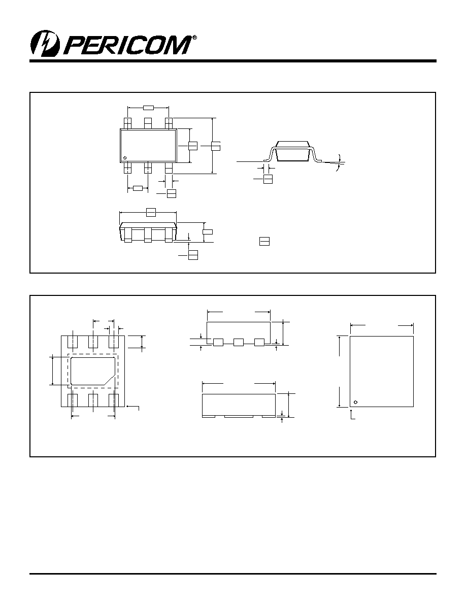
Packaging Mechanical: 6-Pin TDFN (ZC)
0.102
0.118
BSC
0.60
0.000
0.005
0.00
0.15
0.014
0.019
0.35
0.50
1.50
1.75
0.059
0.068
0.10
0.023
0.004
1.45MAX.
SEATING
PLANE
0.057
0∫ - 10∫
1.90
0.075
0.037
BSC
2.60
3.00
0.95
0.110
0.118
2.80
3.00
X.XX
X.XX
Datum "A"
DENOTES DIMENSIONS
IN MILLIMETERS
2
5
3
6
4
Packaging Mechanical: 6-Pin SOT-23(T)
0.0 - 0.05
0.20 REF.
2.00 ± 0.10
2.30 ± 0.10
0.40 ± 0.10
1.40 ± 0.10
2.00 ± 0.10
2.30 ± 0.10
0.80 MAX.
0.0 - 0.05
0.80 MAX.
0.30 ± 0.05
0.65 BSC
Pin #1
Pin #1
0.90 ± 0.10
10
PS8634C 09/13/04
PI5A3159
SOT
INY
TM
1 Low-Voltage
SPDT Analog Switch
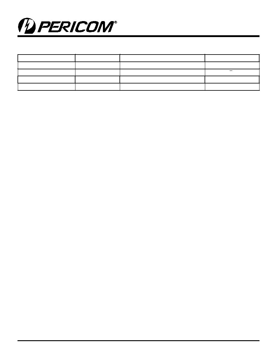
Ordering Information
Ordering Code
Package Code
Package Description
Top Marking
PI5A3159TX
T
6-pin SOT-23
ZL
PI5A3159TEX
T
6-pin SOT-23
ZL
PI5A3159ZCX
(1)
ZC
6-contact TDFN
ZL
PI5A3159ZCEX
ZC
Pb-free & Green 6-contact TDFN
ZL
Notes:
1. This product has always shipped as only a lead free product, but since it was introduced prior to Pericom's strategy of adding an E to all Green/
Lead free parts many customers order it without the E suffix. Please migrate new designs and qualification to include the E suffix. Pericom at
this point in time will continue to offer devices marked both ways, but may at a later date eliminate the non-E part number.
2. Thermal Characteristics can be found on the world wide web at www.pericom.com/packaging/
3. Number of transistors : 753
4. X = Tape and reel
Pericom Semiconductor Corporation ∑ 1-800-435-2336 ∑ www.pericom.com