 | –≠–ª–µ–∫—Ç—Ä–æ–Ω–Ω—ã–π –∫–æ–º–ø–æ–Ω–µ–Ω—Ç: PI5A319AP | –°–∫–∞—á–∞—Ç—å:  PDF PDF  ZIP ZIP |
2 5
PS7059B 02/23/98
PI5A317A/318A/319A
Precision Wide Bandwidth Analog Switches
Features
∑
Single-Supply Operation (+2V to +6V)
∑
Rail-to-Rail Analog Signal Dynamic Range
∑
Low On-Resistance (6
typ with 5V supply)
Minimizes Distortion and Error Voltages
∑
On-Resistance Matching Channels, 0.8
typ
∑
On-Resistance Flatness, 3
typ
∑
Low Charge Injection Reduces Glitch Errors. Q = 4pC typ
∑
Replaces Mechanical Relays
∑
High Speed. t
ON
= 10ns typ
∑
Low Off-Isolation: -72dB@1MHz
∑
Wide -3dB Bandwidth: 170 MHz
∑
High-Current Channel Capability: >100mA
∑
TTL/CMOS Logic Compatible
∑
Low Power Consumption (0.5
µ
W typ)
∑
Pin-compatible with DG41X, MAX31X
Applications
∑
Audio, Video Switching and Routing
∑
Battery-Powered Communication Systems
∑
Computer Peripherals
∑
Telecommunications
∑
Portable Instrumentation
Functional Diagram, Pin Configuration and Truth Table
Switches shown for Logic 0 input
NC = Normally Open, NO = Normally Closed, NIC = Not Internally Connected
For free samples and the latest data sheet visit: www.pericom.com, or phone 1 800-435-2336
Ordering Information
12345678901234567890123456789012123456789012345678901234567890121234567890123456789012345678901212345678901234567890123456789012123456789012
12345678901234567890123456789012123456789012345678901234567890121234567890123456789012345678901212345678901234567890123456789012123456789012
Description
The PI5A317A/381A/319A are analog switches designed for single-
supply operation. These high-precision device is ideal for low-
distortion audio, video, signal switching and routing.
The PI5A317A is a single-pole single-throw (SPST), normally
closed (NC) switch. The PI5A318A has the same pinout but is a
single-pole, single-throw (SPST, normally open (NO) function. The
PI5A319A is a single-pole, double-throw (SPDT) switch
Each switch conducts current equally well in either direction when
on. When off, they block voltages up toV
CC
.
The PI5A317A/381A/319A are fully specified with +5V and +3.3V
supplies. With +5V, theyt guarantee <10
on-resistance. On-resis-
tance matching between channels is within 2
. On-resistance
flatness is less than 5
over the specified range. This switch family
also guarantees fast switching speeds (t
ON
< 20ns).
These products are available in a 8-pin narrow body SOIC, and
PDIP packages for operation over the industrial (-40
o
C to +85
o
C)
temperature range.
r
e
b
m
u
N
t
r
a
P
e
g
a
k
c
a
P
P
A
7
1
3
A
5
I
P
P
I
D
P
n
i
P
-
8
W
A
7
1
3
A
5
I
P
8
-
C
I
O
S
y
d
o
B
w
o
rr
a
N
P
A
8
1
3
A
5
I
P
P
I
D
P
n
i
P
-
8
W
A
8
1
3
A
5
I
P
8
-
C
I
O
S
y
d
o
B
w
o
rr
a
N
P
A
9
1
3
A
5
I
P
P
I
D
P
n
i
P
-
8
W
A
9
1
3
A
5
I
P
8
-
C
I
O
S
y
d
o
B
w
o
rr
a
N
NC (NO, 318)
COM
PI5A317A
1
NIC
NIC 2
IN
GND 3
NIC
V
4
6
5
7
8
cc
NO
COM 1
NIC
NC 2
IN
GND
PI5A319A
3
NIC
V
4
6
5
7
8
cc
N
I
A
7
1
3
A
5
I
P
A
8
1
3
A
5
I
P
0
N
O
F
F
O
1
F
F
O
N
O
N
I
1
W
S
2
W
S
0
N
O
F
F
O
1
F
F
O
N
O
2 6
PS7059B 02/23/98
12345678901234567890123456789012123456789012345678901234567890121234567890123456789012345678901212345678901234567890123456789012123456789012
12345678901234567890123456789012123456789012345678901234567890121234567890123456789012345678901212345678901234567890123456789012123456789012
PI5A317A/318A/319A
Precison Wide Bandwidth Analog Switches
Single 5.0V Supply
DC Electrical Characteristics
(Over the Operating Range, T
A
= ≠40∞C to +85∞C, V
CC
= 5V ±10%, GND = 0V)
Parameters
Description
Test Conditions
(1)
Min.
Typ
(2)
Max.
Units
V
ANALOG
Analog Signal Range
(2)
0
--
5
V
R
ON
ON-Resistance
I
NC
or
NO
= 10 mA to 30 mA
--
6
12
R
ON
Match Between Channels
(319A)
--
0.8
2
R
FLAT(ON)
R
ON
Flatness
(4)
I
ON
= 1 mA, V
NO
, V
NC
= 0V to V
CC
--
3
5
I
NO(OFF)
Off Leakage Current
V
NO
, V
NC
= 4.5V
≠80
--
80
nA
I
NC(ON)
I
COM(ON)
On Leakage Current
V
NO
, V
NC
= 4.5V
≠30
--
30
nA
I
O
Output Current
V
NO
, V
NC
or V
COM
= 0V to V
CC
100
--
--
mA
V
IH
Input HIGH Voltage
Guaranteed Logic HIGH Level
2.0
--
--
V
V
IL
Input LOW Voltage
Guaranteed Logic LOW Level
≠0.5
--
0.8
V
I
IH
Input HIGH Current
V
CC
= Max., V
IN
= V
CC
--
--
±1
µA
I
IL
Input LOW Current
V
CC
= Max., V
IN
= GND
--
--
±1
µA
I
CC
Quiescent Supply Current
Vcc = 5.5V, Vin = 0V or Vcc
--
--
1
µA
Storage Temperature ................................................................... ≠65∞C to +150∞C
Ambient Temperature with Power Applied .................................. ≠40∞C to +85∞C
Supply Voltage to Ground Potential (Inputs & Vcc Only) ............. ≠0.5V to +7.0V
Supply Voltage to Ground Potential (Outputs & D/O Only) .......... ≠0.5V to +7.0V
DC Input Voltage ...................................................................... ≠0.5V to Vcc+0.5V
DC Output Current .................................................................................... 120 mA
Power Dissipation .......................................................................................... 0.5W
Note:
Stresses greater than those listed under
MAXIMUM RATINGS may cause permanent
damage to the device. This is a stress rating only
and functional operation of the device at these
or any other conditions above those indicated in
the operational sections of this specification is
not implied. Exposure to absolute maximum rating
conditions for extended periods may affect
reliability.
Dynamic Electrical Characteristics
(Over the Operating Range, T
A
= ≠40∞C to +85∞C, V
CC
= 5V ±10%, GND = 0V)
Parameters
Description
Test Conditions
(1)
Min.
Typ
(2)
Max.
Units
t
ON
Turn-on Time
V
COM
= 3.0V, see Figure 1
--
10
20
ns
t
OFF
Turn-off Time
V
COM
= 3.0V, see Figure 1
--
4
10
ns
Q
Charge Injection
(2)
C
L
= 0.5 nF, V
Gen
= 0V, see Figure 4
--
3
5
pC
C(
OFF
)
NC or NO Capacitance
f = 1 kHz
--
13
--
pF
C
COM
(
ON
/
OFF
)
COM On Capacitance
f = 1 kHz (319A)
--
45
--
pF
C
COM
(
OFF
)
COM Off Capacitance
f = 1 kHz (317A, 318A)
--
13
--
pF
OIRR
Off Isolation
R
L
= 100
, f = 1 MHz, see Figure 2
--
-
72
--
dB
BW
Bandwidth ≠3 dB
R
L
= 100
(319)
, see Figure 3
--
106
--
MHz
R
L
= 100
(317, 318),
see Figure 3
--
200
--
MHz
D
Distortion R
FLAT
/R
L
R
L
= 100
--
4
--
%
Maximum Ratings
(Above which the useful life may be impaired. For user guidelines, not tested.)
Notes:
1. For Max or Min. conditions, use appropriate value specified under Electrical Characteristics for applicable device type.
2. Guaranteed by design.
2 7
PS7059B 02/23/98
12345678901234567890123456789012123456789012345678901234567890121234567890123456789012345678901212345678901234567890123456789012123456789012
12345678901234567890123456789012123456789012345678901234567890121234567890123456789012345678901212345678901234567890123456789012123456789012
PI5A317A/318A/319A
Precison Wide Bandwidth Analog Switches
Single 3.3V Supply
DC Electrical Characteristics
(Over the Operating Range, T
A
= ≠40∞C to +85∞C, V
CC
= 3.3V ±10%, GND = 0V)
Dynamic Electrical Characteristics
(Over the Operating Range, T
A
= ≠40∞C to +85∞C, V
CC
= 3.3V ±10%, GND = 0V)
Parameters
Description
Test Conditions
(1)
Min.
Typ
(2)
Max.
Units
t
ON
Turn-on Time
V
COM
= 3.0V, see Figure 1
--
28
40
ns
t
OFF
Turn-off Time
V
COM
= 3.0V, see Figure 1
--
4
20
ns
Q
Charge Injection
(2)
C
L
= 1.0 nF, V
Gen
= 0V, see Figure 4
--
3
5
pC
C(
OFF
)
NC or NO Capacitance
f = 1 kHz
--
15
--
pF
C
COM
(
ON
/
OFF
) COM On/Off Capacitance
f = 1 kHz (319)
--
50
--
pF
C
COM
(
OFF
)
COM Off Capacitance
f = 1 kHz (317, 318)
--
15
--
pF
OIRR
Off Isolation
R
L
= 100
, f = 1 MHz, see Figure 2
--
72
--
dB
BW
Bandwidth ≠3 dB
R
L
= 100
(319), see Figure 3
--
90
--
MHz
R
L
= 100
(317, 318), see Figure 3
--
200
--
MHz
D
Distortion
R
L
= 100
--
4
--
%
Notes:
1. For Max. or Min. conditions, use appropriate value specified under Electrical Characteristics for applicable device type.
2. Guaranteed by design.
s
r
e
t
e
m
a
r
a
P
n
o
it
p
i
r
c
s
e
D
s
n
o
it
i
d
n
o
C
t
s
e
T
)
1
(
.
n
i
M
)
2
(
p
y
T
.
x
a
M
s
ti
n
U
V
ANALOG
e
g
n
a
R
l
a
n
g
i
S
g
o
l
a
n
A
0
V
CC
V
R
ON
e
c
n
a
t
si
s
e
R
-
N
O
I
ON
A
m
0
3
o
t
A
m
0
1
=
8
1
2
2
n
o
R
)
3
(
sl
e
n
n
a
h
C
n
e
e
w
t
e
B
h
c
t
a
M
1
3
R
FLAT
(
ON
)
R
ON
s
s
e
n
t
al
F
I
ON
V
,
A
m
1
=
NO
V
,
NC
V
o
t
V
0
=
CC
7
.
8
5
.
2
1
I
NO
(
OFF
)
I
NC
(
ON
)
t
n
e
rr
u
C
e
g
a
k
a
e
L
ff
O
V
NO
V
,
NC
V
0
.
3
=
0
8
0
8
A
n
I
COM
(
ON
)
t
n
e
rr
u
C
e
g
a
k
a
e
L
n
O
V
NO
V
,
NC
V
0
.
3
=
0
8
0
8
I
O
t
n
e
rr
u
C
t
u
p
t
u
O
V
NO
V
,
NC
V
r
o
COM
V
o
t
V
0
=
CC
0
8
A
m
V
IH
e
g
a
tl
o
V
H
G
I
H
t
u
p
n
I
l
e
v
e
L
H
G
I
H
ci
g
o
L
d
e
e
t
n
a
r
a
u
G
0
.
2
V
V
IL
e
g
a
tl
o
V
W
O
L
t
u
p
n
I
l
e
v
e
L
W
O
L
ci
g
o
L
d
e
e
t
n
a
r
a
u
G
5
.
0
8
.
0
I
IH
t
n
e
rr
u
C
H
G
I
H
t
u
p
n
I
V
CC
V
,.
x
a
M
=
IN
V
=
CC
1
±
A
µ
I
IL
t
n
e
rr
u
C
W
O
L
t
u
p
n
I
V
CC
V
,.
x
a
M
=
IN
D
N
G
=
1
±
I
CC
t
n
e
rr
u
C
y
l
p
p
u
S
t
n
e
c
s
ei
u
Q
V
CC
V
,.
x
a
M
=
IN
V
r
o
V
0
=
CC
1
2 8
PS7059B 02/23/98
12345678901234567890123456789012123456789012345678901234567890121234567890123456789012345678901212345678901234567890123456789012123456789012
12345678901234567890123456789012123456789012345678901234567890121234567890123456789012345678901212345678901234567890123456789012123456789012
PI5A317A/318A/319A
Precison Wide Bandwidth Analog Switches
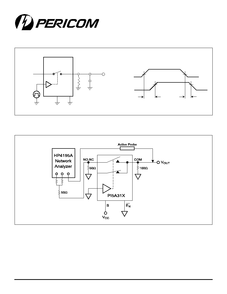
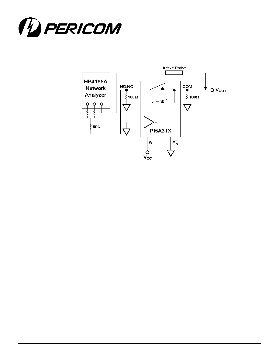
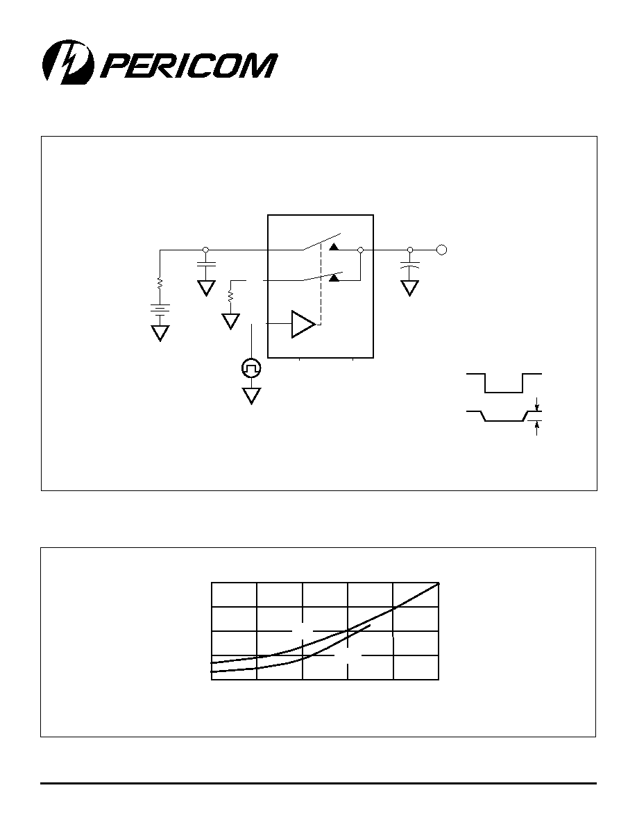
NC, NO
3V
IN
PI5A31X
COM
100
W
V
OUT
15 pF
Test Circuits
Figure 2. Off Isolation
DIGITAL
INPUT
ANALOG
OUTPUT
50%
50%
90%
90%
tON
tOFF
Figure 1. Switching Time
2 9
PS7059B 02/23/98
12345678901234567890123456789012123456789012345678901234567890121234567890123456789012345678901212345678901234567890123456789012123456789012
12345678901234567890123456789012123456789012345678901234567890121234567890123456789012345678901212345678901234567890123456789012123456789012
PI5A317A/318A/319A
Precison Wide Bandwidth Analog Switches
Figure 3. Bandwidth
Typical Operating Characteristics
3 0
PS7059B 02/23/98
12345678901234567890123456789012123456789012345678901234567890121234567890123456789012345678901212345678901234567890123456789012123456789012
12345678901234567890123456789012123456789012345678901234567890121234567890123456789012345678901212345678901234567890123456789012123456789012
PI5A317A/318A/319A
Precison Wide Bandwidth Analog Switches
Figure 5. Charge Injection
Vcc
50
0.01
R
GEN
E
IN
GND
V
GEN
V
O
PI5A100
C
L
1 nF
Polystyrene
COM
NC
S
Freq = 100KHz
DC = 50%
V
GEN
= 0V
R
GEN
= 0
3V
AV
O
V
OUT
SELECT
OFF ON OFF
NO,NC
PI5A31X
IN
IN
NC
0.5 nF
Polystyrene
0.01
µ
F
Figure 6. Charge Injection vs Analog Voltage
0
5
10
15
20
0
2
3
1
4
5
3.3V
5V
Voltage In (Volts)
Charge Injection
(
P
C
)
V
CC
= +5V,
3.3V
T
A
= 25∞C
CL = 0.5 nF
3 1
PS7059B 02/23/98
12345678901234567890123456789012123456789012345678901234567890121234567890123456789012345678901212345678901234567890123456789012123456789012
12345678901234567890123456789012123456789012345678901234567890121234567890123456789012345678901212345678901234567890123456789012123456789012
PI5A317A/318A/319A
Precison Wide Bandwidth Analog Switches
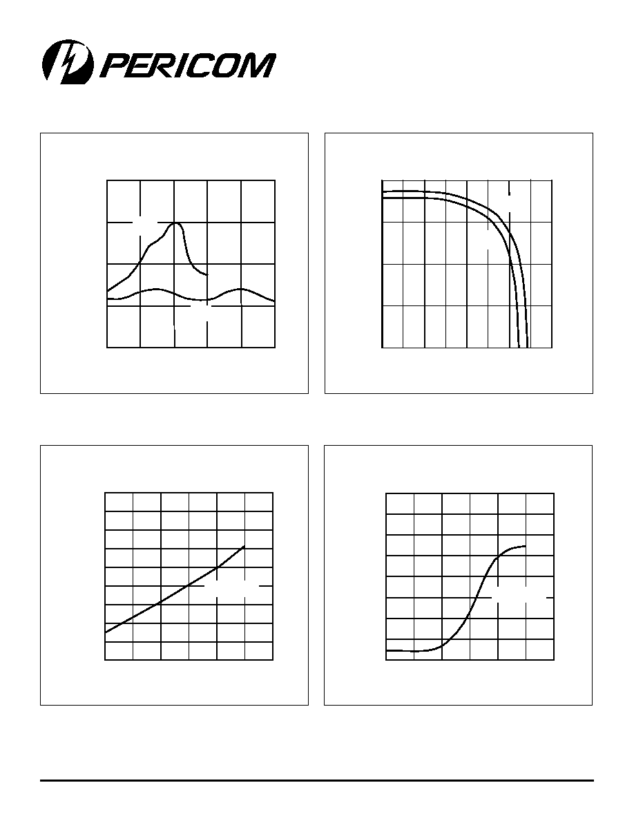
Figure 7. On-Resistance vs. Input Voltage
Figure 8. Insertion Loss vs. Frequency
Figure 9. Off Isolation vs. Frequency
Figure 10. Crosstalk vs Frequency
0
5
10
15
20
0
2
3
1
4
5
3.3V
5V
-4
-3
-2
-1
0
1K
1M
10M
100M
1G
3.3V
5V
0
-10
-20
-30
-40
-50
-60
-70
-80
-90
1M
10M
100M
1G
3.3V, 5V
0
-10
-20
-30
-40
-50
-60
-70
-80
1M
10M
100M
1G
3.3V, 5V
R
L
= 100
T
A
= 25∞C
R
IN
= 1dBm
R
L
= 100
T
A
= 25∞C
P
IN
= 1dBm
T
A
= 25∞C
R
L
= 100
P
IN
= 1dBm
T
A
= 25∞C
R
L
= 100
Input Voltage (V)
Frequency (Hz)
Frequency (Hz)
Frequency (Hz)
On-Resistance R
ON
(
)
Crosstalk XTALK (dB)
Off Isolation OIRR (dB)
Insertion Loss BW (dB)
Pericom Semiconductor Corporation
2380 Bering Drive ∑ San Jose, CA 95131 ∑ 1-800-435-2336 ∑ Fax (408) 435-1100 ∑ http://www.pericom.com