 | –≠–ª–µ–∫—Ç—Ä–æ–Ω–Ω—ã–π –∫–æ–º–ø–æ–Ω–µ–Ω—Ç: PI5A392AQ | –°–∫–∞—á–∞—Ç—å:  PDF PDF  ZIP ZIP |
1
PS7080G 12/10/02
12345678901234567890123456789012123456789012345678901234567890121234567890123456789012345678901212345678901234567890123456789012123456789012
12345678901234567890123456789012123456789012345678901234567890121234567890123456789012345678901212345678901234567890123456789012123456789012
14
15
16
9
13
12
11
10
1
2
3
4
5
7
6
8
IN1
COM1
NC1
N.C.
GND
NC4
IN4
COM4
IN2
NC2
V
N.C.
NC3
COM3
IN3
COM2
PS391
CC
14
15
16
9
13
12
11
10
1
2
3
4
5
7
6
8
IN1
COM1
NO1
N.C.
GND
NO4
IN4
COM4
IN2
NO2
V
N.C.
NO3
COM3
IN3
COM2
PS392
CC
14
15
16
9
13
12
11
10
1
2
3
4
5
7
6
8
IN1
COM1
NO1
N.C.
GND
NO4
IN4
COM4
IN2
NC2
V
N.C.
NC3
COM3
IN3
COM2
PS393
CC
A
2
9
3
A
5
I
P
c
i
g
o
L
h
c
t
i
w
S
0
1
F
F
O
N
O
A
3
9
3
A
5
I
P
c
i
g
o
L
4
,
1
s
e
h
c
t
i
w
S
3
,
2
s
e
h
c
t
i
w
S
0
1
F
F
O
N
O
N
O
F
F
O
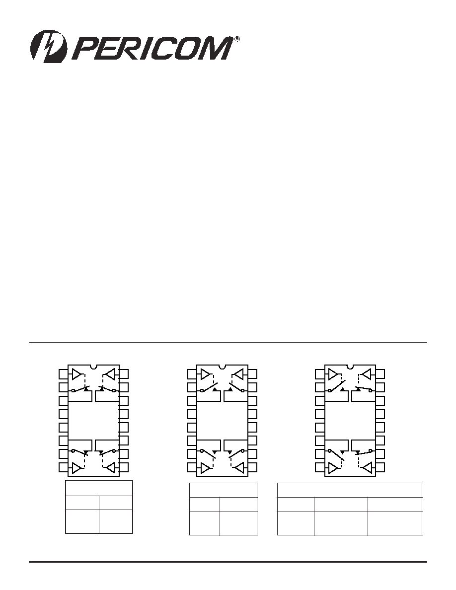
PI5A391A
PI5A392A
PI5A393A
Functional Diagram, Pin Configuration and Truth Tables
Precision Wide
Bandwidth Quad Analog Switches
Switches are shown with logic "0" input.
PI5A391A
PI5A392A
PI5A393A
Features
∑
Single-Supply Operation (+2V to +6V)
∑
Rail-to-Rail Analog Signal Range
∑
Low On-Resistance (6ohm typ @ 5V)
Minimizes Distortion and Error Voltages
∑
R
ON
Matching Between Channels, 0.4 ohm typ
∑
On-Resistance Flatness, 2ohm typ
∑
Low Charge Injection. Q=4pC typ.
Reduces Step errors, "clicking, popping" noise
∑
High Speed. t
ON
, 10ns typ
∑
Very Low Crosstalk: -72dB @ 30 MHz
∑
Wide -3dB Bandwidth: >200 MHz
∑
High-Current Channel Capability: >100mA
∑
TTL/CMOS Logic Compatible
∑
Low Power Consumption (0.5µW typ)
∑
Pin-compatible with DG3XX, DG4XX, MAX39X
Applications
∑
Audio, Video Switching and Routing
∑
Battery-Powered Communication Systems
∑
Computer Peripherals
∑
Telecommunications
∑
Portable Instrumentation
∑
Mechanical Relay Replacement
Description
The PI5A391A/392A/393A are monolithic analog switches de-
signed for low-voltage, single-supply operation. These high-preci-
sion devices are ideal for low-distortion audio, video, signal switch-
ing and routing applications.
The PI5A391A is a quad single-pole single-throw (SPST), normally
closed (NC) switch. The PI5A392A has four normally open (NO)
switches. The PI5A393A has two NC and two NO switches per
package.
Each switch conducts current equally well in either direction when
on. When off they block voltages up to the power-supply rails.
The PI5A391A/392A/393A are fully specified with +5V, and +3.3V
supplies. With +5V, they guarantee <12-ohm on-resistance. On-
resistance matching between channels is within 2-ohm.
On-resistance flatness is less than 4ohm over the full signal range.
The PI5A39X family guarantees fast switching speeds (t
ON
< 20ns).
These products are available in the 16-pin narrow-body SOIC, and
QSOP packages for operation over the industrial (-40
o
C to +85
o
C)
temperature range.
1
9
3
A
5
I
P
c
i
g
o
L
h
c
t
i
w
S
0
1
N
O
F
F
O
12345678901234567890123456789012123456789012345678901234567890121234567890123456789012345678901212345678901234567890123456789012123456789012
12345678901234567890123456789012123456789012345678901234567890121234567890123456789012345678901212345678901234567890123456789012123456789012
PI5A391A, PI5A392A , PI5A393A
Precision Wide Bandwidth Quad Analog Switches
2
PS7080G 12/10/02
Storage Temperature ......................................................... ≠65∞C to +150∞C
Ambient Temperature with Power Applied ............................ ≠40∞C to +85∞C
Supply Voltage to Ground Potential ....................................... ≠0.5V to +7.0V
DC Input Voltage .............................................................. ≠0.5V to Vcc+0.5V
DC Output Current ............................................................................. 120 mA
Power Dissipation .................................................................................. 0.5W
Note:
Stresses greater than those listed under MAXIMUM
RATINGS may cause permanent damage to the
device. This is a stress rating only and functional
operation of the device at these or any other conditions
above those indicated in the operational sections of
this specification is not implied. Exposure to abso-
lute maximum rating conditions for extended
periods may affect reliability.
Single 5.0V Supply
DC Electrical Characteristics
(Over the Operating Range, T
A
= ≠40∞C to +85∞C, V
CC
= 5V ±10%, GND = 0V)
Parameters Description
Test Conditions
(1)
Min.
Typ
(2)
Max.
Units
V
ANALOG
Analog Signal Range
0
--
V
CC
V
R
ON
ON-Resistance
I
NC
or
NO
= 10 mA to 30 mA
--
6
18
ohm
R
ON
Match Between Channels
--
0.4
2
ohm
R
FLAT(ON)
R
ON
Flatness
I
ON
= 1 mA, V
NO
, V
NC
= 0V
TO
5V
--
1
2
ohm
I
NO(OFF)
On/Off Leakage Current
V
NO
, V
NC
= 4.5V
≠30
--
30
nA
I
NC(ON)
I
CC
Quiescent Supply Current
V
CC
= 5.5V, V
IN
= 0V
OR
V
CC
--
--
100
nA
I
O
Output Current
V
NO
, V
NC
or V
COM
= 0V to 5V
100
--
--
mA
V
IH
Input HIGH Voltage
Guaranteed Logic HIGH Level
2.0
--
--
V
V
IL
Input LOW Voltage
Guaranteed Logic LOW Level
≠0.5
--
0.8
V
I
IH
Input HIGH Current
V
CC
= Max., V
IN
= V
CC
--
--
±1
µA
I
IL
Input LOW Current
V
CC
= Max., V
IN
= GND
--
--
±1
µA
Notes:
1. For Max. or Min. conditions, use appropriate value specified under Electrical Characteristics for applicable device type.
2. Guaranteed by design.
Maximum Ratings
(Above which the useful life may be impaired. For user guidelines, not tested.)
12345678901234567890123456789012123456789012345678901234567890121234567890123456789012345678901212345678901234567890123456789012123456789012
12345678901234567890123456789012123456789012345678901234567890121234567890123456789012345678901212345678901234567890123456789012123456789012
PI5A391A, PI5A392A , PI5A393A
Precision Wide Bandwidth Quad Analog Switches
3
PS7080G 12/10/02
Dynamic Electrical Characteristics
(Over the Operating Range, T
A
= ≠40∞C to +85∞C, V
CC
= 5V ±10%, GND = 0V)
Parameters Description
Test Conditions
(1)
Min.
Typ
(2)
Max.
Units
t
ON
Turn-on Time
V
COM
= 3.0V, see Figure 1
--
10
20
ns
t
OFF
Turn-off Time
V
COM
= 3.0V, see Figure 1
--
5
10
ns
X
TALK
Crosstalk
R
L
= 100 ohm, f = 30 MHz, see Figure 4
--
≠72
--
dB
C
(OFF)
NC or NO Capacitance
f = 1 kHz
--
13
--
pF
OIRR
Off Isolation
R
L
= 100
ohm, f = 30 MHz, see Figure 5
--
≠55
--
dB
BW
Bandwidth ≠3 dB
R
L
= 100
ohm, see Figure 3
--
200
--
MHz
D
Distortion
R
ON
/R
L
R
L
= 100
ohm
--
2
--
%
Q
Charge Injection
C
L
= 1 nF, V
Gen
= 0V
--
3
5
pC
Single 3.3V Supply
DC Electrical Characteristics
(1)
(Over the Operating Range, T
A
= ≠40∞C to +85∞C, V
CC
= 3.3V ±10%, GND = 0V)
Parameters Description
Test Conditions
(1)
Min.
Typ
(2)
Max.
Units
V
ANALOG
Analog Signal Range
0
--
V
CC
V
R
ON
ON-Resistance
I
ON
= 10 mA to 30 mA
--
15
28
R
ON
Match Between Channels
--
0.4
2
R
FLAT(ON)
R
ON
Flatness
I
ON
= 1 mA, V
NO
, V
NC
= 0V
TO
5V
--
1
2
I
NO(OFF)
On/Off Leakage Current
V
NO
, V
NC
= 4.5V
≠30
--
30
nA
I
NC(ON)
I
CC
Quiescent Supply Current
V
CC
= 5.5V, V
IN
= 0V
OR
V
CC
--
--
100
nA
I
O
Output Current
V
NO
, V
NC
or V
COM
= 0V to 5V
80
--
--
mA
V
IH
Input HIGH Voltage
Guaranteed Logic HIGH Level
2.0
--
--
V
V
IL
Input LOW Voltage
Guaranteed Logic LOW Level
≠0.5
--
0.8
V
I
IH
Input HIGH Current
V
CC
= Max., V
IN
= V
CC
--
--
±1
µA
I
IL
Input LOW Current
V
CC
= Max., V
IN
= GND
--
--
±1
µA
Notes:
1. For conditions shown as Max or Min, use appropriate value specified under Electrical Characteristics for applicable device type.
2. Guaranteed by design.
3.
R
ON
=
R
ON
max
≠
R
ON
min.
4. Flatness is defined as the difference between the maximum and minimum value of on-resistance as measured over the specified
analog signal range.
Dynamic Electrical Characteristics
(Over the Operating Range, T
A
= ≠40∞C to +85∞C, V
CC
= 3.3V ±10%, GND = 0V)
Parameters Description
Test Conditions
(1)
Min.
Typ
(2)
Max.
Units
t
ON
Turn-on Time
V
COM
= 3.0V, see Figure 1
--
20
40
ns
t
OFF
Turn-off Time
V
COM
= 3.0V, see Figure 1
--
10
20
ns
X
TALK
Crosstalk
RL = 100 ohm, f = 30 MHz, see Figure 4
--
≠72
--
dB
C
(OFF)
NC or NO Capacitance
f = 1 kHz
--
15
--
pF
OIRR
Off Isolation
R
L
= 100
ohm, f = 30 MHz, see Figure 5
--
≠55
--
dB
BW
Bandwidth ≠3 dB
R
L
= 100
ohm, see Figure 3
--
190
--
MHz
D
Distortion
R
ON
/R
L
R
L
= 100ohm
--
2
--
%
Q
Charge Injection
C
L
= 1 nF, V
Gen
= 0V
--
3
10
pC
12345678901234567890123456789012123456789012345678901234567890121234567890123456789012345678901212345678901234567890123456789012123456789012
12345678901234567890123456789012123456789012345678901234567890121234567890123456789012345678901212345678901234567890123456789012123456789012
PI5A391A, PI5A392A , PI5A393A
Precision Wide Bandwidth Quad Analog Switches
4
PS7080G 12/10/02
The 5A39X can be used to insert various capacitors (C1, C2) and set proper RC
times for integration. Resistors R
1
and R
2
set initial gain. The R
IN
resistor X C1
or C2 sets the RC time. The reset switch discharges the hold capacitor through
R
IN
.
Applications
Figure 1. Programmable Integrator and Sample/Hold
+
VOUT
C2
C1
Integrate Reset/
Hold
PS391
RIN
VIN
R1
R2
C1
C2
12345678901234567890123456789012123456789012345678901234567890121234567890123456789012345678901212345678901234567890123456789012123456789012
12345678901234567890123456789012123456789012345678901234567890121234567890123456789012345678901212345678901234567890123456789012123456789012
PI5A391A, PI5A392A , PI5A393A
Precision Wide Bandwidth Quad Analog Switches
5
PS7080G 12/10/02
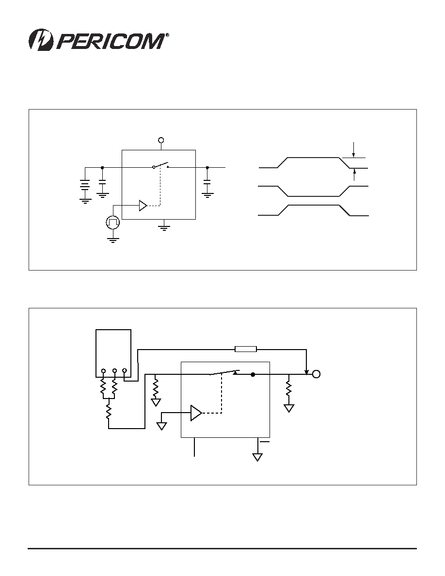
Test Circuits
Figure 2. Switching Time
Figure 3. Bandwidth
V
+
+5V
GND
IN
IN
OFF
ON
ON
OFF
OFF
OFF
COM
IN
C
L
V
OUT
Q = (
VOUT) (CL)
1nF
.1
µ
F
NO or NC
V
V
Logic
Input
V
GEN
OUT
OUT
S
DUT
PI5A39X
COM
NO,NC
I
N
E
N
V
CC
100
µ
V
OUT
HP4195A
Network
Analyser
50
µ
Active Probe
100
µ
12345678901234567890123456789012123456789012345678901234567890121234567890123456789012345678901212345678901234567890123456789012123456789012
12345678901234567890123456789012123456789012345678901234567890121234567890123456789012345678901212345678901234567890123456789012123456789012
PI5A391A, PI5A392A , PI5A393A
Precision Wide Bandwidth Quad Analog Switches
6
PS7080G 12/10/02
S
PI5A39X
COM
E
N
V
CC
100
µ
V
OUT
HP4195A
Network
Analyser
50
µ
Active Probe
50
µ
NO,NC
Figure 4. Crosstalk
Typical Operating Characteristics
Figure 5. Off Isolation
S
PI5A39X
COM
E
N
V
CC
100
µ
HP4195A
Network
Analyser
50
µ
Active Probe
100
µ
NO,NC
RL=100
µ
V
OUT
COM
12345678901234567890123456789012123456789012345678901234567890121234567890123456789012345678901212345678901234567890123456789012123456789012
12345678901234567890123456789012123456789012345678901234567890121234567890123456789012345678901212345678901234567890123456789012123456789012
PI5A391A, PI5A392A , PI5A393A
Precision Wide Bandwidth Quad Analog Switches
7
PS7080G 12/10/02
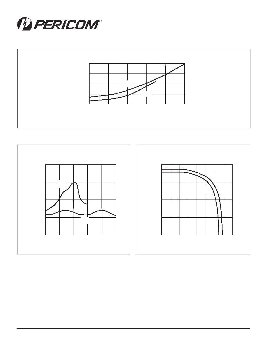
Figure 6. Charge Injection vs Voltage In
0
5
10
15
20
0
2
3
1
4
5
3.3V
5V
V
CC
= +5V,
3.3V
T
A
= 25∞C
CL = 1nF
Voltage In (Volts)
Charge Injection
(
P
C
)
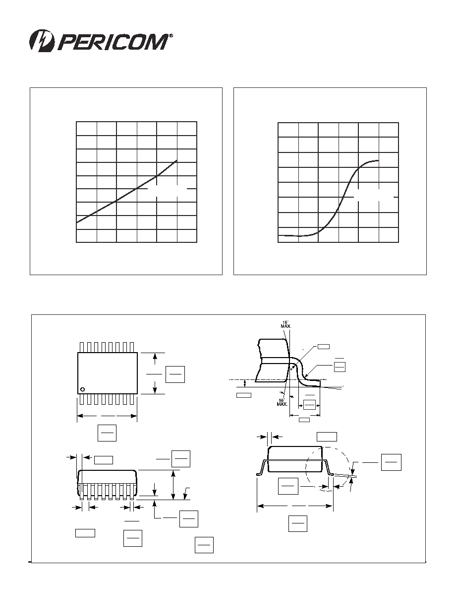
Figure 7. On-Resistance vs Input Voltage
Figure 8. Insertion Loss vs Frequency
0
5
10
15
20
0
2
3
1
4
5
3.3V
5V
-4
-3
-2
-1
0
1K
1M
10M
100M
1G
3.3V
5V
R
H
= 100
T
A
= 25∞C
R
IN
= 1dBm
R
L
= 100
T
A
= 25∞C
Input Voltage (V)
Frequency (Hz)
On-Resistance
R
ON
(
)
Insertion Loss BW (dB)
12345678901234567890123456789012123456789012345678901234567890121234567890123456789012345678901212345678901234567890123456789012123456789012
12345678901234567890123456789012123456789012345678901234567890121234567890123456789012345678901212345678901234567890123456789012123456789012
PI5A391A, PI5A392A , PI5A393A
Precision Wide Bandwidth Quad Analog Switches
8
PS7080G 12/10/02
Figure 9. Off Isolation vs Frequency
Figure 10. Crosstalk vs Frequency
0
-10
-20
-30
-40
-50
-60
-70
-80
-90
1M
10M
100M
1G
3.3V, 5V
0
-10
-20
-30
-40
-50
-60
-70
-80
1M
10M
100M
1G
3.3V, 5V
P
IN
= 1dBm
T
A
= 25∞C
R
L
= 100
P
IN
= 1dBm
T
A
= 25∞C
R
L
= 100
Frequency (Hz)
Frequency (Hz)
Crosstalk XTALK (dB)
Off Isolation OIRR (dB)
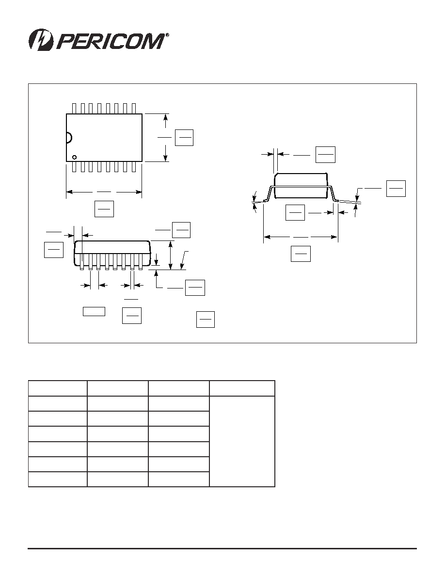
Packaging Mechanical: 16-Pin, QSOP
.189
.197
.053
.069
.004
.010
SEATING
PLANE
.025
BSC
.007
.010
.228
.244
1
16
.150
.157
.016
.050
X.XX
X.XX
DENOTES DIMENSIONS IN MILLIMETERS
0.635
4.80
5.00
1.35
1.75
5.79
6.19
0.101
0.254
.008
.012
0.203
0.305
3.81
3.99
0.178
0.254
0.38
0.41
1.27
.008
0.203
.015 x 45
∞
REF
Detail A
Detail A
.008
0.20
MIN.
Guage Plane
.010
0.254
.041
1.04
REF
.016
.035
0.41
0.89
0∞-6∞
.008
.013
0.20
0.33
12345678901234567890123456789012123456789012345678901234567890121234567890123456789012345678901212345678901234567890123456789012123456789012
12345678901234567890123456789012123456789012345678901234567890121234567890123456789012345678901212345678901234567890123456789012123456789012
PI5A391A, PI5A392A , PI5A393A
Precision Wide Bandwidth Quad Analog Switches
9
PS7080G 12/10/02
SEATING PLANE
.050
BSC
1
16
0-8∞
.149
.157
X.XX
X.XX
DENOTES DIMENSIONS
IN MILLIMETERS
3.78
3.99
.386
.393
9.80
10.00
1.27
.053
.068
1.35
1.75
.2284
.2440
5.80
6.20
.0040
.0098
0.10
0.25
.013
.020
.0155
.0260
0.330
0.508
0.393
0.660
.0075
.0098
0.25
0.50
.0099
.0196
x 45∞
0.19
0.25
.016
.050
0.41
1.27
REF
Packaging Mechanical: 16-Pin, SOIC
Ordering Information
r
e
b
m
u
N
t
r
a
P
e
g
a
k
c
a
P
e
d
o
C
e
g
a
k
c
a
P
e
r
u
t
a
r
e
p
m
e
T
Q
A
1
9
3
A
5
I
P
P
O
S
Q
,
n
i
P
-
6
1
6
1
Q
C
∞
5
8
+
o
t
C
∞
0
4
≠
W
A
1
9
3
A
5
I
P
C
I
O
S
,
n
i
P
-
6
1
6
1
W
Q
A
2
9
3
A
5
I
P
P
O
S
Q
,
n
i
P
-
6
1
6
1
Q
W
A
2
9
3
A
5
I
P
C
I
O
S
,
n
i
P
-
6
1
6
1
W
Q
A
3
9
3
A
5
I
P
P
O
S
Q
,
n
i
P
-
6
1
6
1
Q
W
A
3
9
3
A
5
I
P
C
I
O
S
,
n
i
P
-
6
1
6
1
W
Pericom Semiconductor Corporation
2380 Bering Drive ∑ San Jose, CA 95131 ∑ 1-800-435-2336 ∑ Fax (408) 435-1100 ∑ http://www.pericom.com