 | –≠–ª–µ–∫—Ç—Ä–æ–Ω–Ω—ã–π –∫–æ–º–ø–æ–Ω–µ–Ω—Ç: PI5A4684 | –°–∫–∞—á–∞—Ç—å:  PDF PDF  ZIP ZIP |
1
PS8792B 05/09/06
Features
∑ CMOS Technology for Bus and Analog Applications
∑ Low On-Resistance: 0.5.
∑ Wide V
CC
Range: 1.65V to 5.5V
∑ Rail-to-Rail Signal Range
∑ Control Input Overvoltage Tolerance: 5.5V min.
∑ High Off Isolation: -42dB
∑ Crosstalk Rejection Reduces Signal Distortion: -70dB
∑ Low THD (0.05% @ V
CC
= 2.7V)
∑ Break-Before-Make Switching
∑ Extended Industrial Temperature Range: ≠40
∞
C to 85
∞
C
∑ Packaging (Pb-free & Green):
≠ 10-ball Chip Scale Packaging (CSP)
Applications
∑ Cell Phones
∑ PDAs
∑ MP3 players
∑ Portable Instrumentation
∑ Computer Peripherals
∑ Speaker Headset Switching
∑ Power Routing
∑ Relay Replacement
∑ Audio and Video Signal Routing
∑ PCMCIA Cards
∑ Modems
PI5A4684
Chip Scale Packaging, Dual SPDT Analog Switch
Description
Pericom Semiconductor's PI5A4684 is a dual high-bandwidth,
fast single-pole double throw (SPDT) CMOS switch. It can be
used as an analog switch or as a low-delay bus switch. Specified
over a wide operating power supply voltage, 1.65V to 5.5V, the
PI5A4684 has a maximum On-Resistance of 0.5 at +2.7V.
Break-before-make switching prevents both switches being
enabled simultaneously. This eliminates signal disruption during
switching.
The control input, IN
X
, tolerates input drive signals up to 6.0V,
independent of supply voltage.
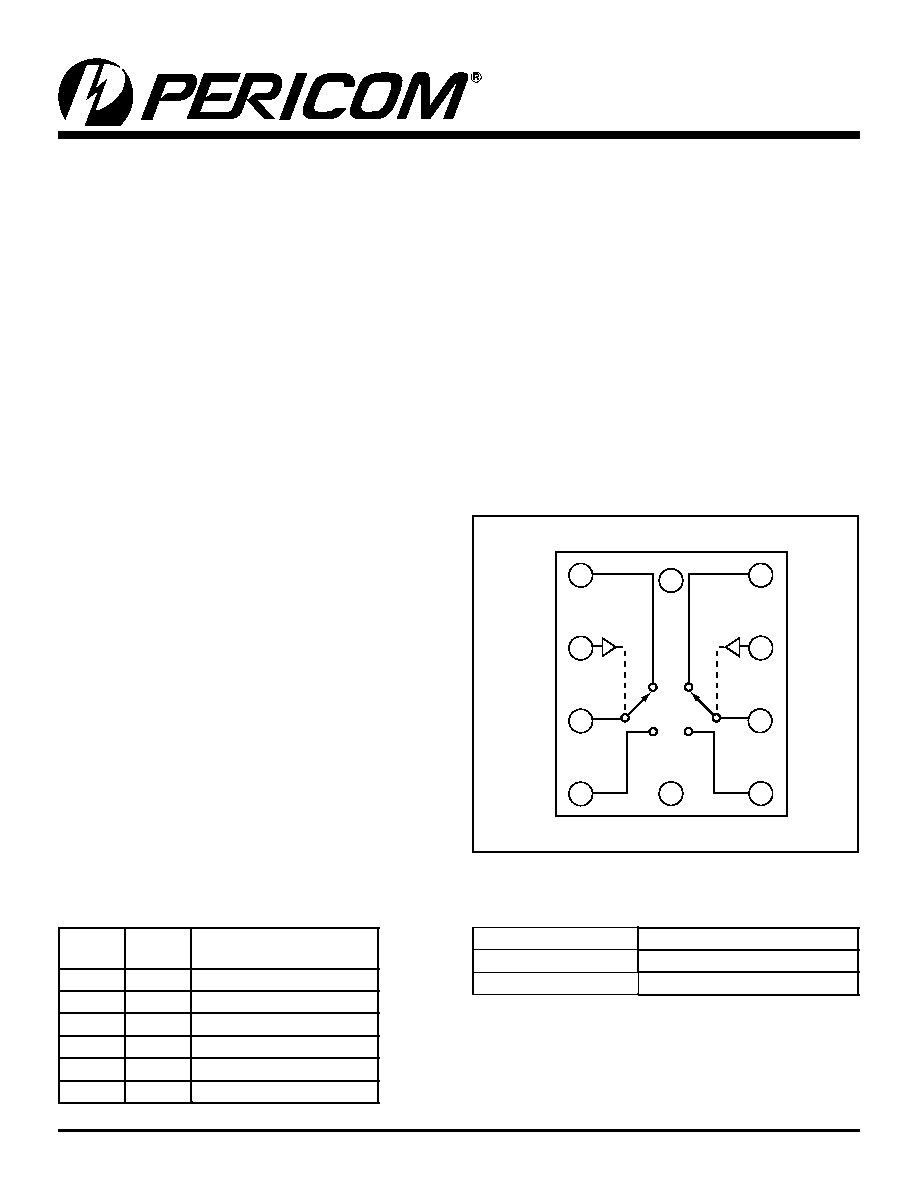
Pin Configuration/ Block Diagram (top view) CSP
IN2
COM1
IN1
COM2
NO2
NC2
NC1
NO1
VCC
GND
C1
C2
C3
C4
B1
B4
C1
C2
A4
A3
A2
A1
Logic Function Table
Logic Input (IN
X
)
Function
0
NC
X
Connected to COM
X
1
NO
X
Connected to COM
X
Pin Description
Pin #
CSP
Name
Description
A4, C4
NO
X
Data Port (Normally open)
B1
GND
Ground
A1, C1
NC
X
Data Port (Normally closed)
A3, C3
COM
X
Common Output / Data Port
B4
V
CC
Postive Power Supply
A2, C2
IN
X
Logic Control
Note:
1. x = 1, or 2
06-0062

2
PS8792B 05/09/06
PI5A4684
Chip Scale Packaging,
Dual SPDT Analog Switch
Recommended Operating Conditions
(3)
Supply Voltage Operating (V
CC
) . . . . . . . . . . . . 1.65V to 5.5V
Control Input Voltage (V
IN
) . . . . . . . . . . . . . . . . . . . 0V to V
CC
Switch Input Voltage (V
IN
). . . . . . . . . . . . . . . . . . . . 0V to V
CC
Output Voltage (V
OUT
) . . . . . . . . . . . . . . . . . . . . . . . 0V to V
CC
Operating Temperature (T
A
) . . . . . . . . . . . . . . . ≠40∞C to +85∞C
Input Rise and Fall Time (t
r
,t
f
)
Control Input V
CC
= 2.3V - 3.6V. . . . . . . . . 0ns/V to 10ns/V
Control Input V
CC
= 4.5V - 5.5V. . . . . . . . . . 0ns/V to 5ns/V
Thermal Resistance (
JA
) . . . . . . . . . . . . . . . . . . . . . . 350∞C/W
Lead Temperature (soldering 10s) . . . . . . . . . . . . . . . . . +300∞C
Bump Temperature (soldering notes)
Infared (15s). . . . . . . . . . . . . . . . . . . . . . . . . . . . . . . . +220∞C
Vapor Phase (60ns) . . . . . . . . . . . . . . . . . . . . . . . . . . +215∞C
Absolute Maximum Ratings
(1)
Supply Voltage V
CC
............................................ ≠0.5V to +7V
DC Switch Voltage (V
S
)
(2)
........................≠0.5V to V
CC
+0.5V
DC Input Voltage (V
IN
)
(2)
................................ ≠0.5V to +7.0V
Continuous Current
NO_NC_COM_
.............................. ±500mA
Peak Current
NO_NC_COM_
(pulsed at 1ms 50% duty cycle) ............................... ±650mA
Peak Current
NO_NC_COM_
(pulsed at 1ms 10% duty cycle) ............................... ±800mA
Storage Temperature Range (T
STG
) .............. ≠65∞C to +150∞C
Junction Temperature under Bias (T
J
) .............................150∞C
Junction Lead Temperature (T
L
)
(Soldering, 10 seconds) ................................................260∞C
Power Dissipation (P
D
) @ +85∞C .................................. 250mW
Notes:
1. "Absolute Maximum Ratings" may cause permanent damage to the device. This is a stress only rating and operation of the device at these or any
other conditions beyond those indicated in the operational sections of this specification is not implied.
2. The input and output negative voltage ratings may be exceeded if the inut and output diode current ratings are observed.
3. Control input must be held HIGH or LOW; it must not float.
06-0062
3
PS8792B 05/09/06
PI5A4684
Chip Scale Packaging,
Dual SPDT Analog Switch
DC Electrical Characteristics +3V Supply
(V
CC
= 2.7V to 3.3V, T
A
= -40 C to + 85 C, unless otherwise noted. Typical values are at 3V and +25∞C.)
Parameter
Symbol
Test Conditions
Min.
Typ.
Max. Units
Analog Switch
Analog Signal Range V
NO
, V
NC
,
V
COM
0
V
CC
V
NC On-Resistance
R
ON(NC)
V
CC
= 2.7V, I
COM
= 100mA,
V
NC
= 0 to V
CC
0.5
0.6
NO On-Resistance
R
ON(NO)
V
CC
= 2.7V, I
COM
= 100mA,
V
NC
= 0 to V
CC
0.4
0.5
On-Resistance Match
Between Channels
R
ON
V
CC
= 2.7V, I
COM
= 100mA,
V
NO
or VNC = 1.5V
0.01
0.06
NC On-Resistance
Flatness
R
ONF(NC)
V
CC
= 2.7V, I
COM
= 100mA,
V
NC
= 0 to V
CC
0.25
NO On-Resistance
Flatness
R
ONF(NO)
V
CC
= 2.7V, I
COM
= 100mA,
V
NO
= 0 to V
CC
0.15
NO or NC Off
Leakage Current
I
OFF (NO)
or
I
OFF (NC)
V
CC
= 3.3V, V
NO
or V
NC
= 3V, 0.3V,
V
COM
= 0.3V, 3V
-80
80
nA
COM On Leakage
Current
I
COM (ON)
V
CC
= 3.3V, V
NO
or V
NC
= 3V, 0.3V,
V
COM
= 0.3V, 3V, or floating
-160
160
Digital I/O
Input Logic High
V
IH
1.3
V
Input Logic Low
V
IL
0.6
Input Hysteresis
V
H
V
CC
= 3.3V
200
mV
IN Input Leakage
Current
I
IN
V
IN
= 0 or V
CC
-1
1
µA
Power Supply
Power-Supply Range V
CC
1.65
5.5
V
Supply Current
I
CC
V
CC
= 5.5V, V
IN
= 0 or V
CC
200
nA
06-0062
4
PS8792B 05/09/06
PI5A4684
Chip Scale Packaging,
Dual SPDT Analog Switch
Capacitance
Parameter
Symbol
Test Conditions
Min.
Typ.
Max.
Units
NC Off Capacitance
C
NC (OFF)
f = 1MHz, See Test Circuit Figure 7.
84
pF
NO Off Capacitance
C
NO (OFF)
f = 1MHz, See Test Circuit Figure 7.
65
NC On Capacitance
C
NC (ON)
f = 1MHz, See Test Circuit Figure 8.
240
NO On Capacitance
C
NO (ON)
f = 1MHz, See Test Circuit Figure 8.
225
Switch and AC Characteristics
(Vcc = 2.7V to 3.3V, Ta = -40 C to +85 C, unless otherwise noted. Typical values are at 3V and +25∞C
Parameter
Symbol
Test Conditions
Min.
Typ.
Max. Units
Turn-On Time
t
ON
V
CC
= 2.7V, V
NO
or V
NC
= 1.5V,
R
L
= 50, C
L
= 35pF,
See Test Circuit Figure 1 & 2.
25
60
ns
Turn-Off Time
t
OFF
V
CC
= 2.7V, V
NO
or V
NC
= 1.5V,
R
L
= 50, C
L
= 35pF,
See Test Circuit Figure 1 & 2.
7
20
Break-Before-Make
Delay
t
BBM
V
CC
= 2.7V, V
NO
or V
NC
= 1.5V,
R
L
= 50, C
L
= 35pF,
See Test Circuit Figure 3.
25
Charge Injection
Q
COM = 0, R
S
= 0, C
L
= 1nF,
See Test Circuit Figure 4.
54
pC
Off-Isolation
O
IRR
C
L
= 5pF, R
L
= 50, f = 100kHz,
V
COM
= 1 V
RMS
, ,
See Test Circuit Figure 5.
-42
dB
Crosstalk
X
TALK
C
L
= 5pF, R
L
= 50, f = 100kHz,
V
COM
= 1 V
RMS
,
See Test Circuit Figure 6.
-70
3dB Bandwidth
f
3dB
See Test Circuit Figure 9.
27
MHz
Total Harmonic
Distortion
THD
R
L
= 32, V
IN
= 3.5V, V
CC
= 4.5V
f = 20Hz to 20kHz
0.07
%
R
L
= 32, V
IN
= 2.0V, V
CC
= 3.4V
f = 20Hz to 20kHz
0.06
R
L
= 32, V
IN
= 1.5V, V
CC
= 2.7V
f = 20Hz to 20kHz
0.05
06-0062
5
PS8792B 05/09/06
PI5A4684
Chip Scale Packaging,
Dual SPDT Analog Switch
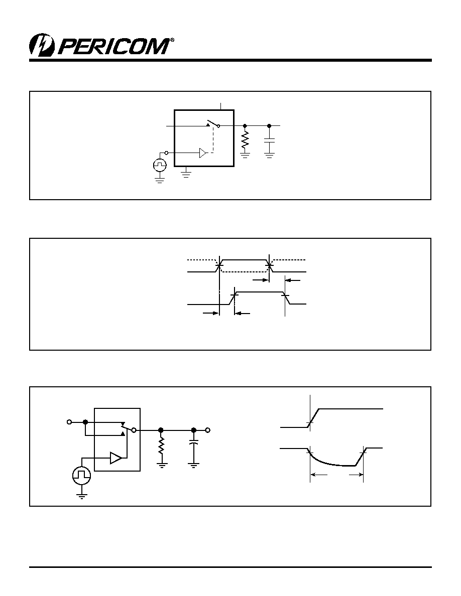
LOGIC
INPUT
R
L
50
COM
GND
IN
C
L
INCLUDES FIXTURE AND STRAY CAPACITANCE.
V
N
NC
or NO
V
CC
C
L
V
CC
V
OUT
35pF
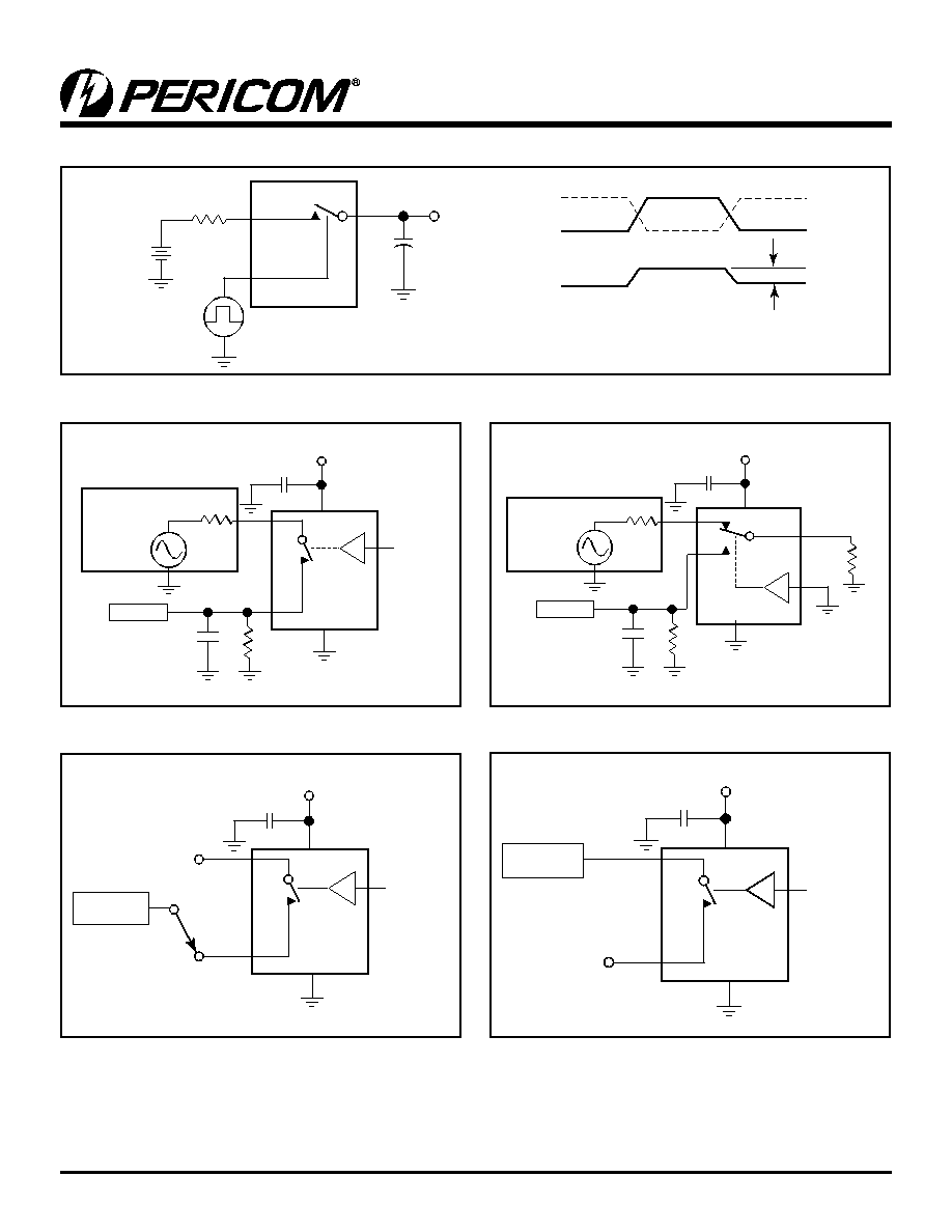
Figure 1. AC Test Circuit
Figure 2. AC Waveforms
Figure 3. Break Before Make Interval Timing
Test Circuits and Timing Diagrams
C
L
35pF
R
L
50
t
BBM
V
OUT
0.9 x V
OUT
Logic
Input
COM
IN
NC
NO
V
IN
Logic
Input
V
OUT
50%
Logic Input Waveforms inverted for
Switches that have opposite logic
* 1.5V for 3.3V Supply
t
ON
V
OUT
t
r
t
f
t
OFF
90%
90%
< 5ns
< 5ns
50%
Switch
Output
Logic
Input
V
IH
V
IL
0V
Off
On
Off
Notes:
1. Unused input (NC or NO) must be grounded.
06-0062
6
PS8792B 05/09/06
PI5A4684
Chip Scale Packaging,
Dual SPDT Analog Switch
Figure 4. Charge Injection Test
C
L
1nF
COM
IN
NC or NO
V
GEN
R
GEN
Logic
Input
Logic
Input
Q = (V
OUT
)(C
L
)
V
OUT
OFF
ON
OFF
V
OUT
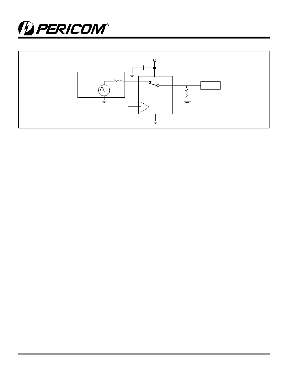
Figure 5. Off Isolation
COM
I
N
10nF
GND
NO
or
NC
V
CC
V
CC
Logic Input
0V or V
IH
RL
50
Signal
Generator
CL
5pF
50
Analyzer
Figure 6. Crosstalk
10nF
GND
V
CC
RL
50
Signal
Generator
CL
5pF
50
Analyzer
COM
NC
NO
V
CC
50
IN
Figure 7. Channel Off Capacitance
Figure 8. Channel On Capacitance
Capacitance
Meter
COM
IN
10nF
GND
f = 1 MHz
NO
or NC
V
CC
V
CC
Logic Input
0V or V
IH
Capacitance
Meter
COM
IN
10nF
GND
NO
V
CC
V
CC
f = 1 MHz
Logic Input
0V or V
IH
or
NC
06-0062
7
PS8792B 05/09/06
PI5A4684
Chip Scale Packaging,
Dual SPDT Analog Switch
Figure 9. Bandwidth
10nF
GND
NC
or
NO
Logic Input
0V or V
IH
IN
V
CC
V
CC
50
Signal
Generator
50
COM
ANALYZER
06-0062
8
PS8792B 05/09/06
PI5A4684
Chip Scale Packaging,
Dual SPDT Analog Switch
Pericom Semiconductor Corporation ∑ 1-800-435-2336 ∑ www.pericom.com
Ordering Information
Ordering Code
Packaging Code
Package Type
PI5A4684GAE
GA
Pb-free & Green, 10-ball CSP
Notes:
∑ Thermal characteristics can be found on the company web site at www.pericom.com/packaging/
∑ E = Pb-free and Green
∑ Adding an X suffix = Tape & Reel
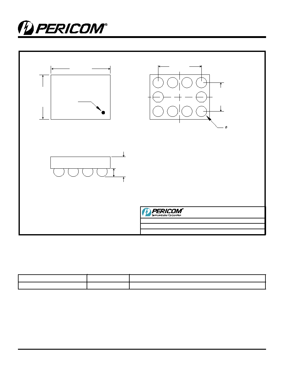
DESCRIPTION: 10-contact CSP (Chip Scale Packaging) without backside coating
PACKAGE CODE: GA (GA10)
DOCUMENT CONTROL #: PD-2048
REVISION: - -
DATE: 11/01/05
06-0062