1
PS7050B 12/09/99
12345678901234567890123456789012123456789012345678901234567890121234567890123456789012345678901212345678901234567890123456789012123456789012
12345678901234567890123456789012123456789012345678901234567890121234567890123456789012345678901212345678901234567890123456789012123456789012
PI5C16211
24-Bit Bus Switch
Product Description
Pericom Semiconductor's PI5C series of logic circuits are produced
using the Company's advanced 0.6 micron CMOS technology.
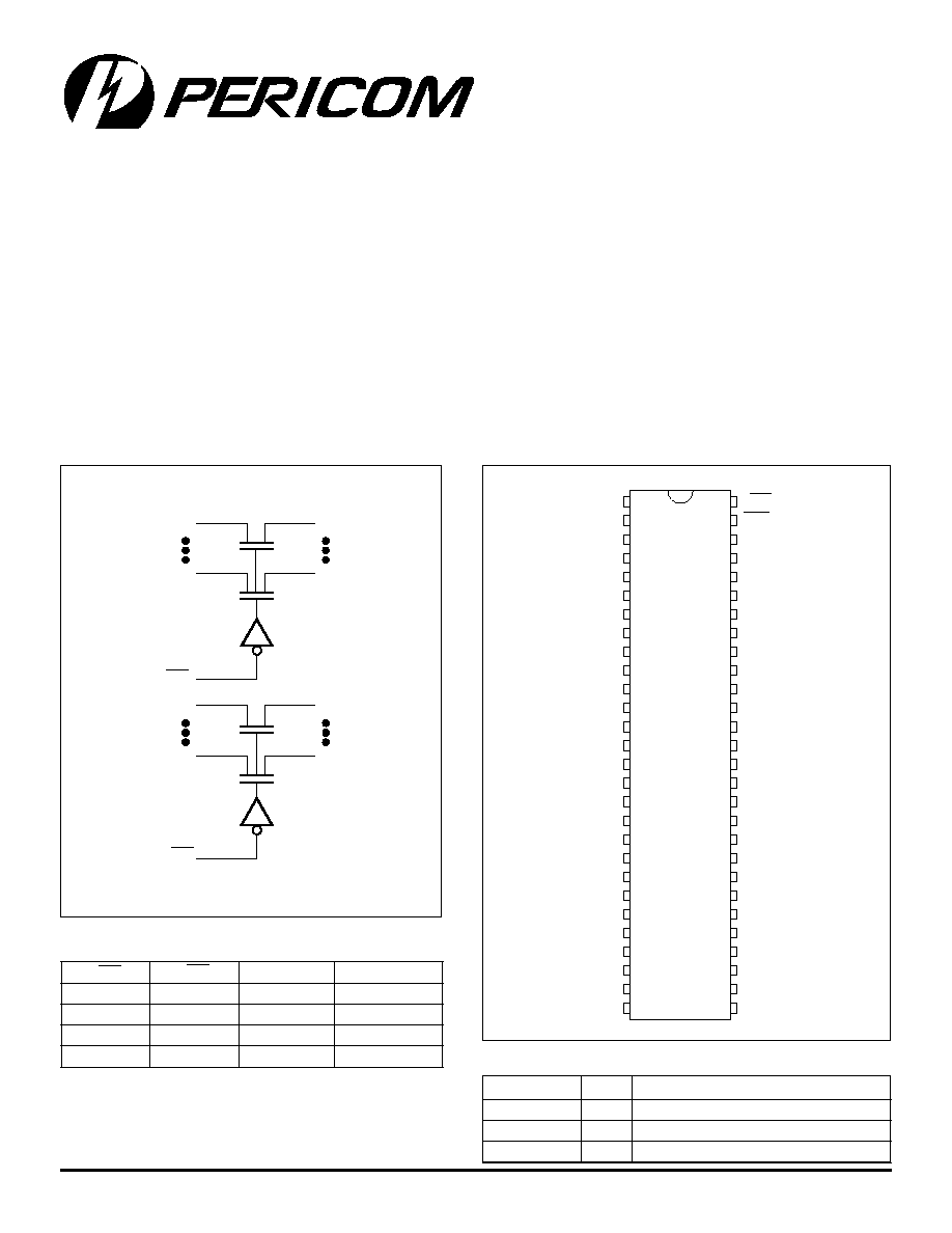
The PI5C16211 is a 24-bit bus switch designed with a low ON
resistance allowing inputs to be connected directly to outputs. This
device operates as a 24-bit or a 12-bit bus switch, which provides
high speed bus switching.
Product Features
∑ Near-zero propagation delay
∑ 5
switches connect inputs to outputs
∑ Direct bus connection when switches are ON
∑ Ultra-low quiescent power (0.2 µA typical) ≠ Ideally
suited for notebook applications
∑ Industrial operating temperature: ≠40∞C to +85∞C
∑ Packages available:
≠ 56-pin 173-mil wide plastic TVSOP (K)
≠ 56-pin 240-mil wide thin plastic TSSOP (A)
≠ 56-pin 300-mil wide plastic SSOP (V)
Logic Block Diagram
Product Pin Configuration
Truth Table
Product Pin Description
Pin Name
I/O
Description
S0-S2
I
Select Inputs
xAx
I/O
Bus A
xB
x
I/O
Bus B
Note:
1. H = High Voltage Level
L = Low Voltage Level
Z = High Impedance
1
2
3
4
5
6
7
8
9
10
11
12
13
14
15
16
17
18
19
20
21
22
23
24
56
55
54
53
52
51
50
49
48
47
46
45
44
43
42
41
40
39
38
37
36
35
34
33
25
26
27
28
32
31
30
29
NC
1
A
1
1
A
2
1
A
3
1
A
4
1
A
5
1
A
6
GND
1
A
7
1
A
8
1
A
9
1
A
10
1
A
11
1
A
12
2
A
1
2
A
2
V
CC
2
A
3
GND
2
A
4
2
A
5
2
A
6
2
A
7
2
A
8
2
A
9
2
A
10
2
A
11
2
A
12
1
OE
1
2
OE
1
B
1
1
B
2
1
B
3
1
B
4
1
B
5
GND
1
B
6
1
B
7
1
B
8
1
B
9
1
B
10
1
B
11
1
B
12
2
B
1
2
B
2
2
B
3
GND
2
B
4
2
B
5
2
B
6
2
B
7
2
B
8
2
B
9
2
B
10
2
B
11
2
B
12
E
O
1
E
O
2
s
O
/
I
B
1
,
A
1
s
O
/
I
B
2
,
A
2
L
L
B
1
=
A
1
B
2
=
A
2
L
H
B
1
=
A
1
Z
H
L
Z
B
2
=
A
2
H
H
Z
Z
56-Pin
A, K,V
1B1
1B12
1A1
1A12
2B1
2B12
2A1
1OE
2OE
2A12
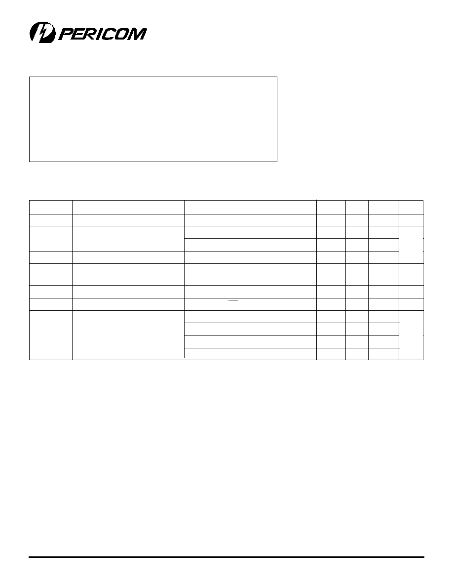
PI5C16211
24-Bit Bus Switch
2
PS7050B 12/09/99
12345678901234567890123456789012123456789012345678901234567890121234567890123456789012345678901212345678901234567890123456789012123456789012
12345678901234567890123456789012123456789012345678901234567890121234567890123456789012345678901212345678901234567890123456789012123456789012
DC Electrical Characteristics
(Over the Operating Range, T
A
= ≠40∞C to +85∞C, V
CC
= 5V ±10%)
Parameters
Description
Test Conditions
Min.
Typ
(1)
Max.
Units
V
IK
Clamp Diode Voltage
V
CC
= 4.5V, I
I
= ≠18mA
--
-- ≠1.2 V
I
I
Input LOW Current
V
CC
= 5.5V, V
I
= V
CC
or GND
--
--
10
V
CC
= 0V, V
I
= 5.5V
--
--
±1
µA
I
CC
Quiescent Power Supply Current
V
CC
= 5.5V, V
I
= V
CC
or GND
--
--
3.0
I
CC
Supply Current per Control Input
V
CC
= 5.5V, One input at 3.4V,
--
--
2.5
mA
@ TTL High
other inputs at V
CC
or GND
C
I
(2)
Control Input Capacitance
V
I
= 3V or 0
--
4.5
--
C
IO
(
OFF
)
(2)
A/B Switch OFF Capacitance
V
O
= 3V or 0,
OE = V
CC
--
5.5
--
R
ON
Switch On Resistance
(3)
V
CC
= 4.0V, V
I
= 2.4V, I
I
= 15 mA
--
14
20
V
CC
= 4.5V, V
I
= 0V, I
I
= 64 mA
--
5
7
V
CC
= 4.5V, V
I
= 0V, I
I
= 30 mA
--
5
7
V
CC
= 4.5V, V
I
= 2.4V, I
I
= 15 mA
--
8
12
Maximum Ratings
(Above which the useful life may be impaired. For user guidelines, not tested.)
Storage Temperature .................................................................... ≠65∞C to +150∞C
Ambient Temperature with Power Applied .................................... ≠40∞C to +85∞C
Supply Voltage to Ground Potential (Inputs & Vcc Only) .............. ≠0.5V to +7.0V
Supply Voltage to Ground Potential (Outputs & D/O Only) ........... ≠0.5V to +7.0V
DC Input Voltage ............................................................................ ≠0.5V to +7.0V
DC Output Current ...................................................................................... 120mA
Power Dissipation .......................................................................................... 1.4W
Note:
Stresses greater than those listed under MAXI-
MUM RATINGS may cause permanent damage
to the device. This is a stress rating only and
functional operation of the device at these or any
other conditions above those indicated in the
operational sections of this specification is not
implied. Exposure to absolute maximum rating
conditions for extended periods may affect reli-
ability.
Notes:
1. Typical values are at V
CC
= 5.0V, T
A
= 25∞C ambient and maximum loading.
2. This parameter is determined by device characterization but is not production tested.
3. Measured by the voltage drop between A and B pin at indicated current through the switch.
ON resistance is determined by the lower of the voltages on the two (A,B) pins.
pF
PI5C16211
24-Bit Bus Switch
3
PS7050B 12/09/99
12345678901234567890123456789012123456789012345678901234567890121234567890123456789012345678901212345678901234567890123456789012123456789012
12345678901234567890123456789012123456789012345678901234567890121234567890123456789012345678901212345678901234567890123456789012123456789012
Note:
1. Typical values are at V
CC
= 5.0V, +25∞C ambient.
Switching Characteristics over Operating Range
Notes:
1. This parameter is guaranteed but not tested on Propagation Delays. The bus switch contributes no propagational delay other than
the RC delay of the ON resistance of the switch and the load capacitance. The time constant for the switch alone is of the order of
0.25ns for 50pF load. Since this time constant is much smaller than the rise/fall times of typical driving signals, it adds very little
propagational delay to the system. Propagational delay of the bus switch when used in a system is determined by the driving
circuit on the driving side of the switch and its interaction with the load on the driven side.
Pericom Semiconductor Corporation
2380 Bering Drive ∑ San Jose, CA 95131 ∑ 1-800-435-2336 ∑ Fax (408) 435-1100 ∑ http://www.pericom.com
Power Supply Characteristics
s
r
e
t
e
m
a
r
a
P
n
o
it
p
i
r
c
s
e
D
.
n
i
M
p
y
T
)
1
(
.
x
a
M
s
ti
n
U
V
C
C
e
g
a
tl
o
V
y
l
p
p
u
S
0
.
4
5
.
5
V
V
H
I
e
g
a
tl
o
V
t
u
p
n
I
l
e
v
e
L
h
g
i
H
0
.
2
V
V
L
I
e
g
a
tl
o
V
t
u
p
n
I
l
e
v
e
L
w
o
L
8
.
0
V
T
A
p
m
e
t
ri
A
-
e
e
r
F
g
n
it
a
r
e
p
O
0
4
-
5
8
C
∞
s
r
e
t
e
m
a
r
a
P
m
o
r
F
)
T
U
P
N
I
(
o
T
)
T
U
P
T
U
O
(
t
s
e
T
s
n
o
it
i
d
n
o
C
V
C
C
V
5
.
0
±
V
5
=
V
C
C
V
4
=
s
ti
n
U
.
n
i
M
.
x
a
M
.
n
i
M
.
x
a
M
t
D
P
)
1
(
B
r
o
A
A
r
o
B
C
L
F
p
0
5
=
R
L
0
0
5
=
5
2
.
0
5
2
.
0
s
n
t
N
E
E
O
B
r
o
A
9
.
3
3
.
9
1
.
0
1
t
S
I
D
E
O
B
r
o
A
3
.
3
5
.
8
1
.
7
t
r
a
P
e
g
a
k
c
a
P
-
n
i
P
e
r
u
t
a
r
e
p
m
e
T
A
1
1
2
6
1
C
5
I
P
)
A
(
P
O
S
S
T
-
6
5
C
∞
5
8
+
o
t
C
∞
0
4
K
1
1
2
6
1
C
5
I
P
)
K
(
P
O
S
S
T
-
6
5
C
∞
5
8
+
o
t
C
∞
0
4
V
1
1
2
6
1
C
5
I
P
)
V
(
P
O
S
S
T
-
6
5
C
∞
5
8
+
o
t
C
∞
0
4
Ordering Information