1
PS7023H 12/18/02
1
2
3
4
5
6
7
GND
8
9
10
11
12
13
14
15
16
17
18
19
20
21
22
23
24
56
55
54
53
52
51
50
49
48
47
46
45
44
43
42
41
40
39
38
37
36
35
34
33
25
26
27
28
32
31
30
29
1 1
A
1 2
A
S
0
2 1
A
2 2
A
3 1
A
3 2
A
4 1
A
4 2
A
5 1
A
5 2
A
6 1
A
6 2
A
V
CC
7 1
A
7 2
A
8 1
A
GND
8 2
A
9 1
A
9 2
A
10 1
A
10 2
A
11 1
A
11 2
A
12 1
A
12 2
A
GND
1 1
B
1 2
B
S
1
2 1
B
2 2
B
3 1
B
3 2
B
4 1
B
4 2
B
5 1
B
5 2
B
6 1
B
6 2
B
7 1
B
7 2
B
8 1
B
GND
8 2
B
9 1
B
9 2
B
10 1
B
10 2
B
11 1
B
11 2
B
12 1
B
12 2
B
S
2
12345678901234567890123456789012123456789012345678901234567890121234567890123456789012345678901212345678901234567890123456789012123456789012
12345678901234567890123456789012123456789012345678901234567890121234567890123456789012345678901212345678901234567890123456789012123456789012
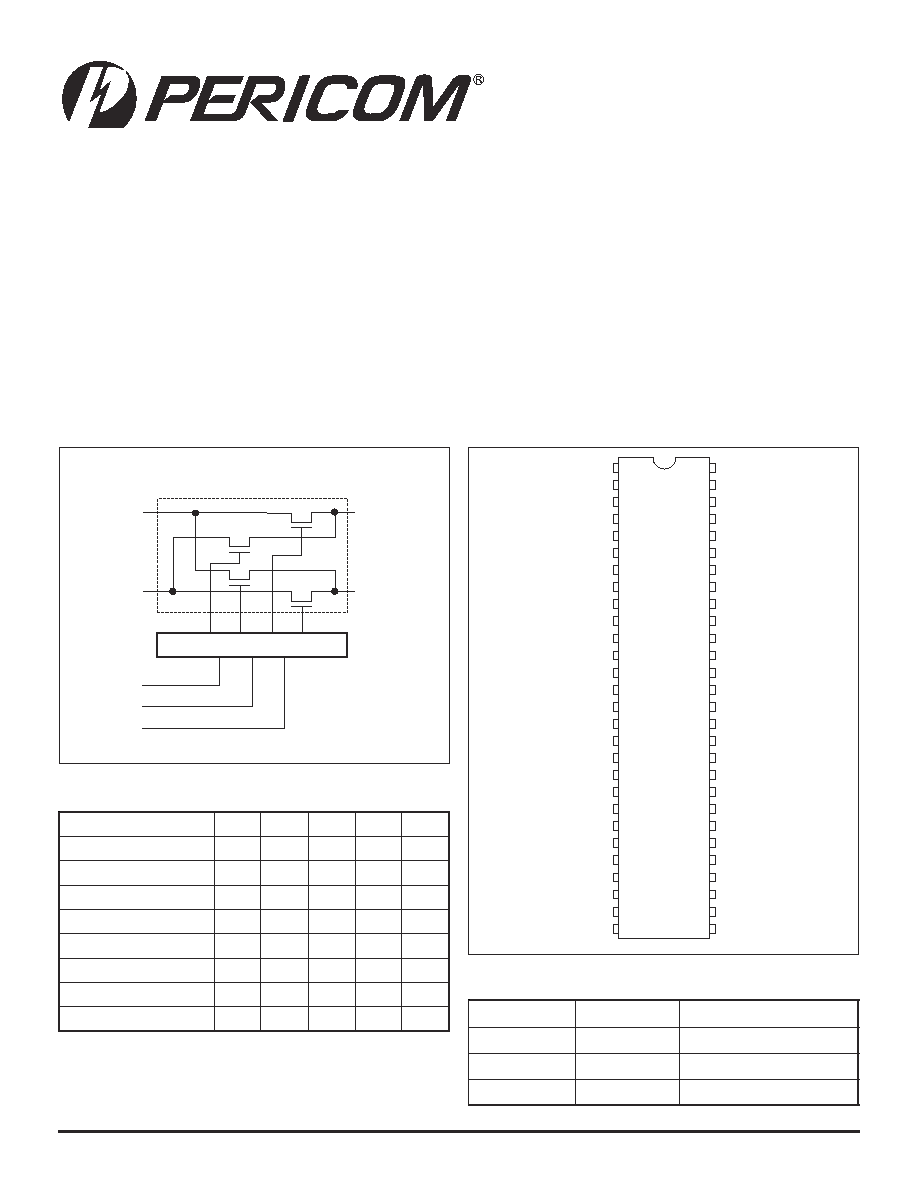
24-Bit Bus Exchange Switch
Product Description
Pericom Semiconductor's PI5C series of logic circuits are produced
using the Company's advanced submicron CMOS technology.
The PI5C16212 and PI5C162212 are 24-bit bus exchange switches
designed with a low ON resistance allowing inputs to be connected
directly to outputs. This device operates as a 24-bit bus switch
or a 12-bit exchanger that provides data exchanging between
the four signal ports via the data select pins (S0-S2).
To reduce noise resulting from reflections, the PI5C162212 has a
built-in 25-ohm series resistor that eliminates the need for an
external terminating resistor.
Product Features
∑ Near-zero propagation delay
∑ 5-ohm switches connect inputs to outputs
∑ Direct bus connection when switches are ON
∑ Ultra-low quiescent power (0.1µA typical)
≠ Ideally suited for notebook applications
∑ Industrial operating temperature: ≠40∞C to +85∞C
∑ Packages available:
≠ 56-pin 240-mil wide thin plastic TSSOP (A)
≠ 56-pin 300-mil wide plastic SSOP (V)
≠ 56-pin 173-mil wide plastic TVSOP (K) - PI5C16212 only
Product Pin Configuration
Logic Block Diagram
Product Pin Description
Note:
1. H = High Voltage Level
L = Low Voltage Level
Z = High Impedance
Truth Table
PI5C16212
PI5C162212 (25
)
n
o
i
t
c
n
u
F
2
S
1
S
0
S
1
A
2
A
t
c
e
n
n
o
c
s
i
D
L
L
L
Z
Z
1
B
o
t
1
A
L
L
H
1
B
Z
2
B
o
t
1
A
L
H
L
2
B
Z
1
B
o
t
2
A
L
H
H
Z
1
B
2
B
o
t
2
A
H
L
L
Z
2
B
t
c
e
n
n
o
c
s
i
D
H
L
H
Z
Z
2
B
o
t
2
A
,
1
B
o
t
1
A
H
H
L
1
B
2
B
1
B
o
t
2
A
,
2
B
o
t
1
A
H
H
H
2
B
1
B
e
m
a
N
n
i
P
O
/
I
n
o
i
t
p
i
r
c
s
e
D
2
S
-
0
S
I
s
t
u
p
n
I
t
c
e
l
e
S
x
A
x
O
/
I
A
s
u
B
x
B
x
O
/
I
B
s
u
B
56-Pin
A, K, V
1 1
A
1 1
B
1 2
A
1 2
B
FLOW CONTROL
ONE OF TWELVE CHANNELS
S
0
S
1
S
2
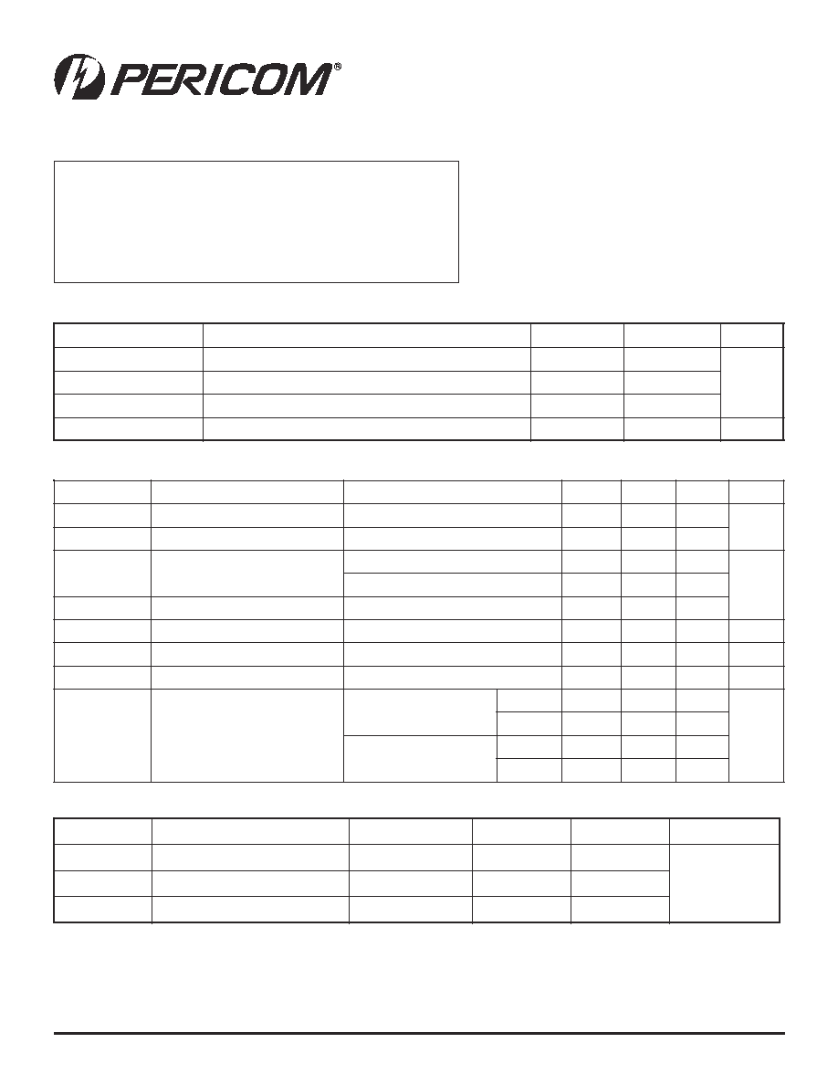
PI5C16212/162212
24-Bit Bus-Exchange Switch
2
PS7023H 12/18/02
12345678901234567890123456789012123456789012345678901234567890121234567890123456789012345678901212345678901234567890123456789012123456789012
12345678901234567890123456789012123456789012345678901234567890121234567890123456789012345678901212345678901234567890123456789012123456789012
Storage Temperature .............................................. ≠65∞C to +150∞C
Ambient Temperature with Power Applied ..............≠40∞C to +85∞C
Supply Voltage to Ground Potential .......................... ≠0.5V to +7.0V
DC Input Voltage ....................................................... ≠0.5V to +7.0V
DC Output Current ................................................................ 120mA
Power Dissipation ....................................................................... 1W
Note:
Stresses greater than those listed under MAXIMUM RATINGS
may cause permanent damage to the device. This is a stress rating
only and functional operation of the device at these or any other
conditions above those indicated in the operational sections of this
specification is not implied. Exposure to absolute maximum rating
conditions for extended periods may affect reliability.
DC Electrical Characteristics
(Over the Operating Range, T
A
= ≠40∞C to +85∞C, V
CC
= 5V ±10%)
Capacitance
(T
A
= 25∞C, f = 1 MHz)
Notes:
1. For Max. or Min. conditions, use appropriate value specified under Electrical Characteristics for the applicable device.
2. Typical values are at V
CC
= 5.0V, T
A
= 25∞C ambient and maximum loading.
3. Not more than one output should be shorted at one time. Duration of the test should not exceed one second.
4. Measured by the voltage drop between A and B pin at indicated current through the switch. ON resistance is determined by the
lower of the voltages on the two (A,B) pins.
5. This parameter is determined by device characterization but is not production tested.
Recommended Operating Condition
Maximum Ratings
(Above which the useful life may be impaired. For user guidelines, not tested.)
r
e
t
e
m
a
r
a
P
n
o
i
t
p
i
r
c
s
e
D
.
n
i
M
.
x
a
M
s
t
i
n
U
V
C
C
e
g
a
tl
o
V
y
l
p
p
u
S
4
5
.
5
V
V
H
I
e
g
a
tl
o
V
t
u
p
n
I
l
e
v
e
L
-
h
g
i
H
2
--
V
L
I
e
g
a
tl
o
V
t
u
p
n
I
l
e
v
e
L
-
w
o
L
--
8
.
0
T
A
e
r
u
t
a
r
e
p
m
e
T
ri
A
-
e
e
r
F
g
n
it
a
r
e
p
O
0
4
≠
5
8
C
∞
s
r
e
t
e
m
a
r
a
P
n
o
i
t
p
i
r
c
s
e
D
s
n
o
i
t
i
d
n
o
C
t
s
e
T
)
1
(
.
n
i
M
p
y
T
)
2
(
.
x
a
M
s
t
i
n
U
V
H
I
e
g
a
tl
o
V
H
G
I
H
t
u
p
n
I
l
e
v
e
L
H
G
I
H
c
i
g
o
L
d
e
e
t
n
a
r
a
u
G
0
.
2
--
--
V
V
L
I
e
g
a
tl
o
V
W
O
L
t
u
p
n
I
l
e
v
e
L
W
O
L
c
i
g
o
L
d
e
e
t
n
a
r
a
u
G
5
.
0
≠
--
8
.
0
I
I
t
n
e
r
r
u
C
t
u
p
n
I
V
C
C
V
,.
x
a
M
=
N
I
V
=
C
C
D
N
G
r
o
--
--
1
±
A
µ
V
C
C
V
,
0
=
N
I
V
=
C
C
--
--
0
1
I
H
Z
O
t
n
e
r
r
u
C
t
u
p
t
u
O
e
c
n
a
d
e
p
m
I
h
g
i
H
V
-
B
,
A
-
0
C
C
--
--
1
±
V
K
I
e
g
a
tl
o
V
e
d
o
i
D
p
m
a
l
C
V
C
C
I
,.
n
i
M
=
N
I
A
m
8
1
≠
=
--
7
.
0
≠
2
.
1
≠
V
I
S
O
t
n
e
r
r
u
C
ti
u
c
ri
C
t
r
o
h
S
)
3
(
V
=
)
A
(
B
,
V
0
=
)
B
(
A
C
C
0
0
1
--
--
A
m
V
H
s
n
i
P
l
o
r
t
n
o
C
t
a
s
i
s
e
r
e
t
s
y
H
t
u
p
n
I
--
0
5
1
--
V
m
R
N
O
e
c
n
a
t
s
i
s
e
R
n
O
h
c
ti
w
S
)
4
(
V
C
C
V
,.
n
i
M
=
N
I
,
V
0
.
0
=
I
N
O
A
m
4
6
=
2
1
2
6
1
--
5
7
2
1
2
2
6
1
0
2
8
2
0
4
V
C
C
V
,.
n
i
M
=
N
I
,
V
4
.
2
=
I
N
O
A
m
5
1
=
2
1
2
6
1
--
--
2
1
2
1
2
2
6
1
0
2
5
3
8
4
s
r
e
t
e
m
a
r
a
P
)
5
(
n
o
i
t
p
i
r
c
s
e
D
s
n
o
i
t
i
d
n
o
C
t
s
e
T
.
p
y
T
.
x
a
M
s
t
i
n
U
C
N
I
e
c
n
a
ti
c
a
p
a
C
t
u
p
n
I
V
N
I
V
0
=
3
6
F
p
C
F
F
O
f
f
O
h
c
ti
w
S
,
e
c
n
a
ti
c
a
p
a
C
B
/
A
V
N
I
V
0
=
6
4
1
C
N
O
n
O
h
c
ti
w
S
,
e
c
n
a
ti
c
a
p
a
C
B
/
A
V
N
I
V
0
=
2
1
0
3
PI5C16212/162212
24-Bit Bus-Exchange Switch
3
PS7023H 12/18/02
12345678901234567890123456789012123456789012345678901234567890121234567890123456789012345678901212345678901234567890123456789012123456789012
12345678901234567890123456789012123456789012345678901234567890121234567890123456789012345678901212345678901234567890123456789012123456789012
Power Supply Characteristics
Notes:
1. For conditions shown as Max. or Min., use appropriate value specified under Electrical Characteristics for applicable device.
2. Typical values are at V
CC
= 5.0V, +25∞C ambient.
3. This is the increase in supply current for each input that is at the specified TTL voltage level rather than V
CC
or GND.
4. Per TTL driven input (V
IN
= 2.7V, control inputs only); A and B pins do not contribute to I
CC
.
5. This current applies to the control inputs only and represent the current required to switch internal capacitance at the specified
frequency. The A and B inputs generate no significant AC or DC currents as they transition. This parameter is not tested, but is
guaranteed by design.
PI5C16212 Switching Characteristics over Operating Range
PI5C162212 Switching Characteristics over Operating Range
Notes:
1. See test circuit and waveforms.
2. This parameter is guaranteed but not tested on Propagation Delays.
3. The bus switch contributes no propagational delay other than the RC delay of the ON resistance of the switch and the load
capacitance. The time constant for the switch alone is of the order of 0.25ns for 50pF load. Since this time constant is much
smaller than the rise/fall times of typical driving signals, it adds very little propagational delay to the system. Propagational delay
of the bus switch when used in a system is determined by the driving circuit on the driving side of the switch and its interaction
with the load on the driven side.
s
r
e
t
e
m
a
r
a
P
n
o
i
t
p
i
r
c
s
e
D
s
n
o
i
t
i
d
n
o
C
t
s
e
T
)
1
(
.
n
i
M
.
p
y
T
)
2
(
.
x
a
M
s
t
i
n
U
I
C
C
t
n
e
r
r
u
C
y
l
p
p
u
S
r
e
w
o
P
t
n
e
c
s
e
i
u
Q
V
C
C
.
x
a
M
=
V
N
I
V
r
o
D
N
G
=
C
C
--
1
.
0
0
.
3
A
µ
I
C
C
)
3
(
H
G
I
H
L
T
T
@
t
u
p
n
I
r
e
p
t
n
e
r
r
u
C
y
l
p
p
u
S
V
C
C
V
5
.
5
=
V
N
I
V
4
.
3
=
)
4
(
--
--
2
.
0
A
m
I
D
C
C
z
H
M
r
e
p
t
u
p
n
I
r
e
p
t
n
e
r
r
u
C
y
l
p
p
u
S
)
5
(
S
N
g
n
il
g
g
o
T
t
u
p
n
I
l
o
r
t
n
o
C
,
D
N
G
=
e
l
c
y
C
y
t
u
D
%
0
5
V
C
C
,.
x
a
M
=
n
e
p
O
s
n
i
P
B
&
A
--
--
5
2
.
0
/
A
m
z
H
M
s
r
e
t
e
m
a
r
a
P
n
o
i
t
p
i
r
c
s
e
D
s
n
o
i
t
i
d
n
o
C
)
1
(
2
1
2
6
1
C
5
I
P
.
m
o
C
.
n
i
M
.
x
a
M
s
t
i
n
U
t
H
L
P
t
L
H
P
y
a
l
e
D
n
o
it
a
g
a
p
o
r
P
)
3
,
2
(
x
A
x
o
t
x
B
x
,
x
B
x
o
t
x
A
x
,
C
L
F
p
0
5
=
R
L
s
m
h
o
0
0
5
=
--
5
2
.
0
s
n
t
H
L
P
t
L
H
P
,
y
a
l
e
D
n
o
it
a
g
a
p
o
r
P
x
B
r
o
x
A
o
t
S
5
.
1
5
.
7
t
H
Z
P
t
L
Z
P
x
B
x
r
o
x
A
x
o
t
S
,
e
m
i
T
e
l
b
a
n
E
s
u
B
5
.
1
0
.
7
t
Z
H
P
t
Z
L
P
x
B
x
r
o
x
A
x
o
t
S
,
e
m
i
T
e
l
b
a
s
i
D
s
u
B
5
.
1
5
.
6
s
r
e
t
e
m
a
r
a
P
n
o
i
t
p
i
r
c
s
e
D
s
n
o
i
t
i
d
n
o
C
)
1
(
2
1
2
2
6
1
C
5
I
P
.
m
o
C
.
n
i
M
.
x
a
M
s
t
i
n
U
t
H
L
P
t
L
H
P
y
a
l
e
D
n
o
it
a
g
a
p
o
r
P
)
3
,
2
(
x
A
x
o
t
x
B
x
,
x
B
x
o
t
x
A
x
,
C
L
F
p
0
5
=
R
L
s
m
h
o
0
0
5
=
--
5
2
.
1
s
n
t
H
Z
P
t
L
Z
P
x
B
x
r
o
x
A
x
o
t
S
,
e
m
i
T
e
l
b
a
n
E
s
u
B
5
.
1
0
.
7
t
Z
H
P
t
Z
L
P
x
B
x
r
o
x
A
x
o
t
S
,
e
m
i
T
e
l
b
a
s
i
D
s
u
B
5
.
1
5
.
6
PI5C16212/162212
24-Bit Bus-Exchange Switch
4
PS7023H 12/18/02
12345678901234567890123456789012123456789012345678901234567890121234567890123456789012345678901212345678901234567890123456789012123456789012
12345678901234567890123456789012123456789012345678901234567890121234567890123456789012345678901212345678901234567890123456789012123456789012
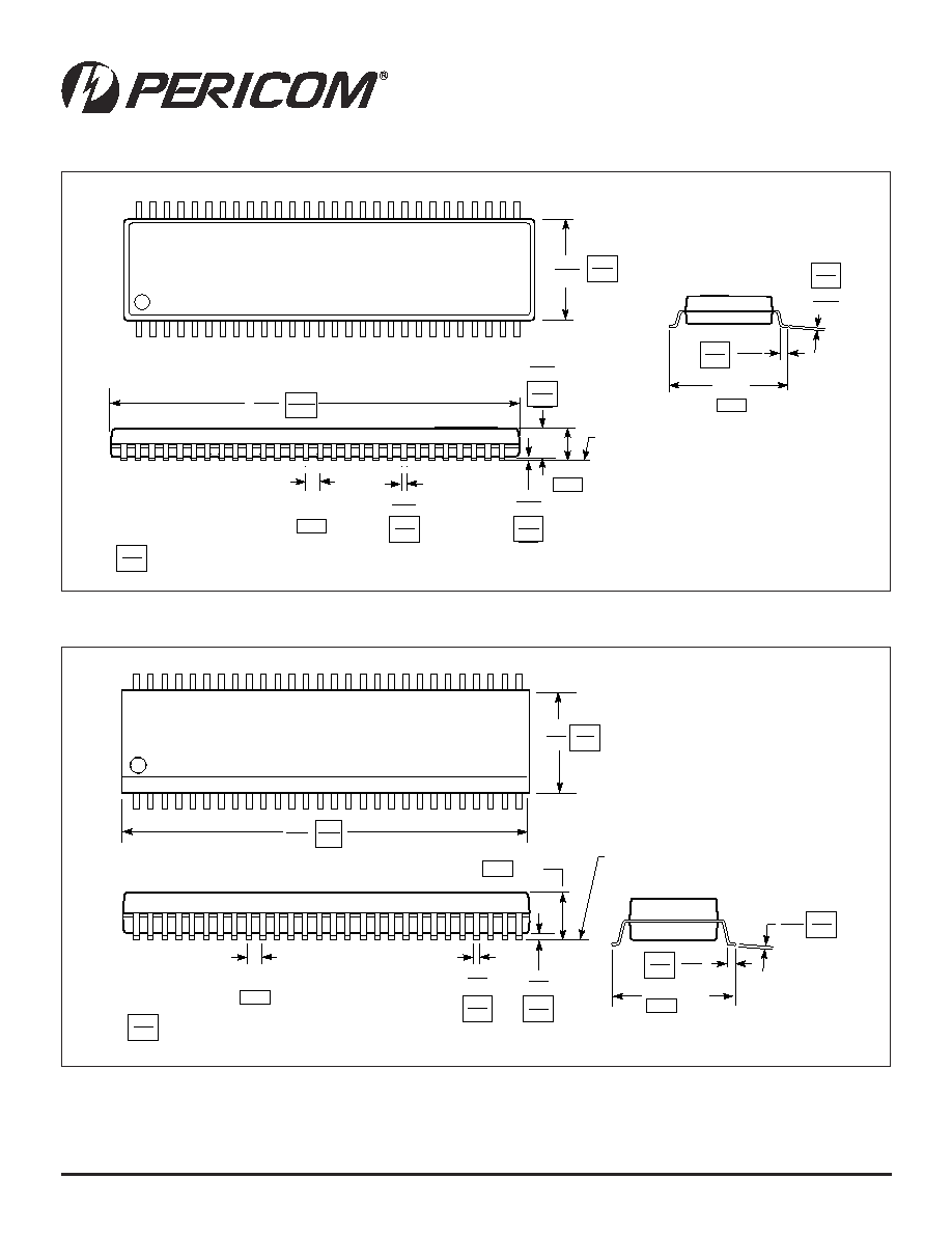
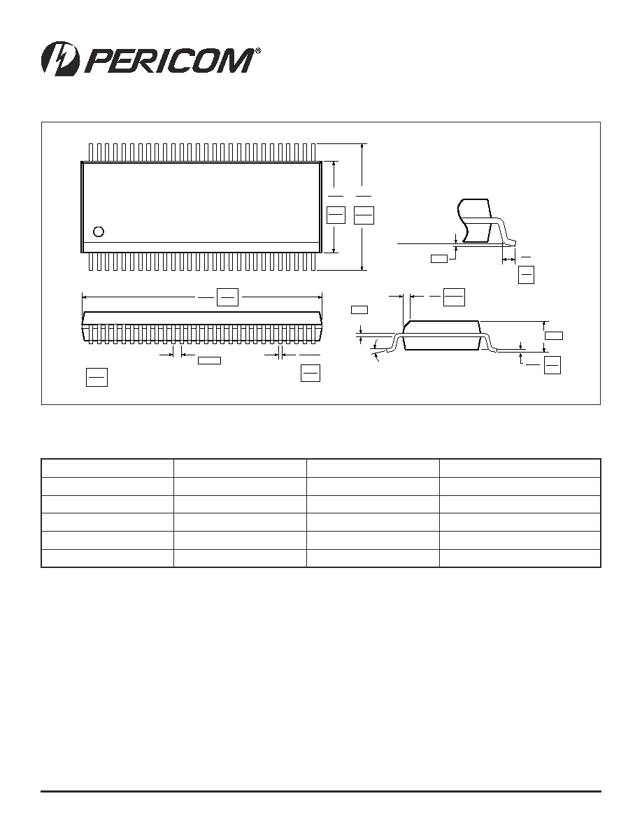
56-Pin 173-Mil Wide Plastic TVSOP (K) Package
56-Pin 240-Mil Wide Thin Plastic TSSOP (A) Package
.047
.031
.041
SEATING
PLANE
.016
BSC
1
56
.169
.177
11.20
11.40
4.30
4.50
1.20
0.40
0.13
0.23
0.80
1.05
X.XX
X.XX
DENOTES DIMENSIONS
IN MILLIMETERS
.002
.006
0.05
0.15
.0035
.008
0.09
0.20
.018
.030
0.45
0.75
6.4
.252
BSC
.005
.009
.441
.449
Max.
.002
.006
SEATING PLANE
.007
.011
.004
.008
1
56
.236
.244
0.50
0.17
0.27
0.05
0.15
0.09
0.20
X.XX
X.XX
DENOTES DIMENSIONS
IN MILLIMETERS
.018
.030
0.45
0.75
.047
Max.
1.20
6.0
6.2
.547
.555
13.9
14.1
.319
8.1
.0197
BSC
BSC
PI5C16212/162212
24-Bit Bus-Exchange Switch
5
PS7023H 12/18/02
12345678901234567890123456789012123456789012345678901234567890121234567890123456789012345678901212345678901234567890123456789012123456789012
12345678901234567890123456789012123456789012345678901234567890121234567890123456789012345678901212345678901234567890123456789012123456789012
Pericom Semiconductor Corporation
2380 Bering Drive ∑ San Jose, CA 95131 ∑ 1-800-435-2336 ∑ Fax (408) 435-1100 ∑ http://www.pericom.com
56-Pin 300-Mil Wide Thin Plastic SSOP (V) Package
Ordering Information
e
d
o
C
g
n
i
r
e
d
r
O
e
m
a
N
e
g
a
k
c
a
P
e
p
y
T
e
g
a
k
c
a
P
e
g
n
a
R
e
r
u
t
a
r
e
p
m
e
T
K
2
1
2
6
1
C
5
I
P
6
5
K
P
O
S
V
T
n
i
p
-
6
5
C
∞
5
8
o
t
0
4
≠
A
2
1
2
6
1
C
5
I
P
6
5
A
P
O
S
S
T
n
i
p
-
6
5
C
∞
5
8
o
t
0
4
≠
A
2
1
2
2
6
1
C
5
I
P
6
5
A
P
O
S
S
T
n
i
p
-
6
5
C
∞
5
8
o
t
0
4
≠
V
2
1
2
6
1
C
5
I
P
6
5
V
P
O
S
S
n
i
p
-
6
5
C
∞
5
8
o
t
0
4
≠
V
2
1
2
2
6
1
C
5
I
P
6
5
V
P
O
S
S
n
i
p
-
6
5
C
∞
5
8
o
t
0
4
≠
0.25
0.20
.025 BSC
0.635
.008
.008
.016
0-8∞
0.20
0.40
.110 2.79
.010
Gauge Plane
.291
.299
X.XX
X.XX
DENOTES DIMENSIONS
IN MILLIMETERS
7.39
7.59
.396
.416
10.06
10.56
.02
.04
0.51
1.01
.015
.025
0.381
0.635
.720
.730
18.29
18.54
.008
.0135
0.20
0.34
1
56
x 45∞
Nom.
Max