1
PS8389A 08/31/99
Product Description
Pericom Semiconductor's PI5C series of logic circuits are produced
using the Company's advanced submicron CMOS technology,
achieving industry leading performance.
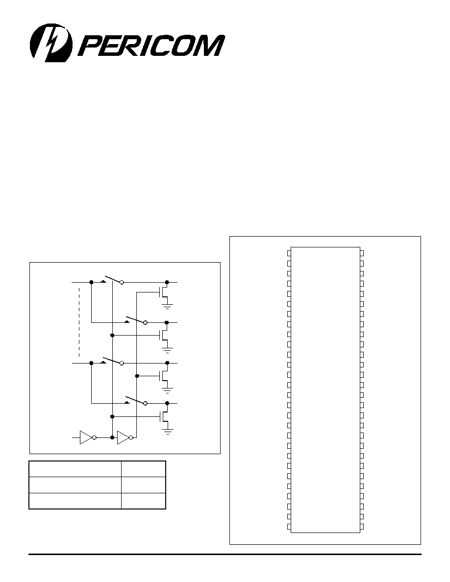
The PI5C16225C is a 12-bit-to-24-bit multiplexer/demultiplexer
bus switch. Industry leading advantages include a propagation
delay of 0.5ns, resulting from 7
channel resistance, and low
I/O capacitance. A port demultiplexes to either B
1
and B
2
. The
switch is bidirectional.
Application
Provides Memory Module Switching.
Logic Block Diagram
Pin Description
PI5C16225C
Low Capacitance 12-Bit-to-24-Bit
Mux/Demux Bus Switch
12345678901234567890123456789012123456789012345678901234567890121234567890123456789012345678901212345678901234567890123456789012123456789012
12345678901234567890123456789012123456789012345678901234567890121234567890123456789012345678901212345678901234567890123456789012123456789012
Product Features
∑
R
ON
is 8
typical
∑
Pulldown on B ports
∑
Low Power: 1mW typical
∑
Industrial Operation Temperature:
-
40∫C to +85∫C
∑
Near Zero propagation delay
∑
Switching speed: 4.5ns max.
∑
Channel on capacitance: 9.0pF (typ.)
∑
V
CC
Operating Range: +4.5V to +5.5V
∑
ESD>2000V . . . Human Body Model
∑
>100 MHz bandwidth (or clock rate)
at 25pF load capacitance
∑
Packages available: 56-pin TSSOP (A)
n
o
it
c
n
u
F
L
E
S
A
n
1
B
n
o
t
1
L
A
n
1
B
n
o
t
2
H
Note:
1. H = High Voltage Level
L = Low Voltage Level
n = 1 to 12
1
2
3
4
5
6
7
GND
8
9
10
11
12
13
14
15
16
17
18
19
20
21
22
23
24
56
55
54
53
52
51
50
49
48
47
46
45
44
43
42
41
40
39
38
37
36
35
34
33
25
26
27
28
32
31
30
29
1
A
1
NC
SEL
2
A
1
NC
3
A
1
NC
4
A
1
NC
5
A
1
NC
6
A
1
NC
V
CC
7
A
1
NC
8
A
1
GND
NC
9
A
1
NC
10
A
1
NC
11
A
1
NC
12
A
1
NC
GND
1
B
1
1
B
2
NC
2
B
1
2
B
2
3
B
1
3
B
2
4
B
1
4
B
2
5
B
1
5
B
2
6
B
1
6
B
2
7
B
1
7
B
2
8
B
1
GND
8
B
2
9
B
1
9
B
2
10
B
1
10
B
2
11
B
1
11
B
2
12
B
1
12
B
2
NC
56-Pin
A
12
B
2
12
A
1
1
A
1
SEL
12
B
1
1
B
2
1
B
1
2
PS8389A 08/31/99
12345678901234567890123456789012123456789012345678901234567890121234567890123456789012345678901212345678901234567890123456789012123456789012
PI5C16225C
Low Capacitance 12-Bit to 24-Bit,
Mux/Demux Bus Switch
Capacitance
(T
A
= 25∞C, f = 1 MHz)
Parameters
(5)
Description
Test Conditions
Typ.
Max.
Units
C
IN
Input Capacitance
V
IN
= 0V
3
--
pF
C
ON
A/B Capacitance, Switch On
V
IN
= 0V
9
11
pF
Storage Temperature ........................................................... ≠65∞C to +150∞C
Ambient Temperature with Power Applied .......................... ≠40∞C to +85∞C
Supply Voltage to Ground Potential (Inputs & Vcc Only) ... ≠0.5V to +7.0V
Supply Voltage to Ground Potential (Outputs & D/O Only) ≠0.5V to +7.0V
DC Input Voltage .................................................................. ≠0.5V to +7.0V
DC Output Current ............................................................................. 120mA
Power Dissipation ................................................................................... 0.5W
Note:
Stresses greater than those listed under MAXIMUM
RATINGS may cause permanent damage to the device.
This is a stress rating only and functional operation of
the device at these or any other conditions above
those indicated in the operational sections of this
specification is not implied. Exposure to absolute
maximum rating conditions for extended periods may
affect reliability.
DC Electrical Characteristics
(Over the Operating Range, T
A
= ≠40∞C to +85∞C, V
CC
= 5V ±10%)
Parameters Description
Test Conditions
(1)
Min.
Typ
(2)
Max.
Units
V
IH
Input HIGH Voltage
Guaranteed Logic HIGH Level
2.0
--
--
V
V
IL
Input LOW Voltage
Guaranteed Logic LOW Level
≠0.5
--
0.8
V
I
IH
Input HIGH Current
V
CC
= Max., V
IN
= V
CC
--
--
±1
µA
I
IL
Input LOW Current
V
CC
= Max., V
IN
= GND
--
--
±1
µA
I
OZ
High Impedance Output Current
B = V
CC
Min., V
CC
= Min.
2.5
--
--
mA
R
ON
Switch On Resistance
(4)
V
CC
= Min., V
IN
= 0.0V,
--
7
12
I
ON
= 12mA
V
CC
= Min., V
IN
= 2.4V,
--
12
23
I
ON
= 8mA
Notes:
1. For Max. or Min. conditions, use appropriate value specified under Electrical Characteristics for the applicable device type.
2. Typical values are at V
CC
= 5.0V, T
A
= 25∞C ambient and maximum loading.
3. Not more than one output should be shorted at one time. Duration of the test should not exceed one second.
4. Measured by the voltage drop between A and B pins at indicated current through the switch. ON resistance is determined by the
lower of the voltages on the two (A & B) pins.
5. This parameter is determined by device characterization but is not production tested.
Maximum Ratings
(Above which the useful life may be impaired. For user guidelines, not tested.)
3
PS8389A 08/31/99
12345678901234567890123456789012123456789012345678901234567890121234567890123456789012345678901212345678901234567890123456789012123456789012
PI5C16225C
Low Capacitance 12-Bit to 24-Bit,
Mux/Demux Bus Switch
PI516225C
Com.
Parameters Description
Conditions
(1)
Min.
Typ.
Max.
Units
t
PLH
Propagation Delay
(2,3)
C
L
= 25pF
0.5
t
PHL
A to B
R
L
= 500
t
PZH
Bus Enable Time
1.3
3.0
4.5
ns
t
PZL
SEL
TO
A,B
t
PHZ
Bus Disable Time
1.3
3.0
4.5
t
PLZ
SEL to A,B
Power Supply Characteristics
Parameters Description
Test Conditions
(1)
Min.
Typ
(2)
Max.
Units
I
CC
Quiescent Power
V
CC
= Max.
V
IN
= GND or V
CC
--
--
200
µA
Supply Current
I
CC
Supply Current per
V
CC
= Max.
V
IN
= 3.4V
(3)
--
--
2.5
mA
Input @ TTL HIGH
other pin=V
CC
or GND
I
CCD
Supply Current per
V
CC
= Max.,
--
--
0.25
mA/
Input per MHz
(4)
A and B Pins Open
MHz
Control Input Toggling
50% Duty Cycle
Notes:
1. For Max. or Min. conditions, use appropriate value specified under Electrical Characteristics for the applicable device.
2. Typical values are at V
CC
= 5.0V, +25∞C ambient.
3. Per TTL driven input (V
IN
= 3.4V, control inputs only); A and B pins do not contribute to I
CC
.
4. This current applies to the control inputs only and represent the current required to switch internal capacitance at the specified
frequency. The A and B inputs generate no significant AC or DC currents as they transition. This parameter is not tested, but is
guaranteed by design.
5. Values for these conditions are examples of the I
CC
formula. These limits are guaranteed but not tested.
Switching Characteristics over Operating Range
Notes:
1. See test circuit and waveforms.
2. This parameter is guaranteed but not tested on Propagation Delays.
3. The bus switch contributes no propagational delay other than the RC delay of the ON resistance of
the switch and the load capacitance. The time constant for the switch alone is of the order of 0.25ns
for 25pF load. Since this time constant is much smaller than the rise/fall times of typical driving
signals, it adds very little propagational delay to the system. Propagational delay of the bus switch
when used in a system is determined by the driving circuit on the driving side of the switch and its
interaction with the load on the driven side.
Pericom Semiconductor Corporation
2380 Bering Drive ∑ San Jose, CA 95131 ∑ 1-800-435-2336 ∑ Fax (408) 435-1100 ∑ http://www.pericom.com
t
r
a
P
e
g
a
k
c
a
P
-
n
i
P
h
t
d
i
W
e
r
u
t
a
r
e
p
m
e
T
A
C
5
2
2
6
1
C
5
I
P
)
6
5
A
(
P
O
S
S
T
-
6
5
li
m
-
0
4
2
C
∞
5
8
+
o
t
C
∞
0
4
Ordering Information