1
PS8362E 03/10/05
Description
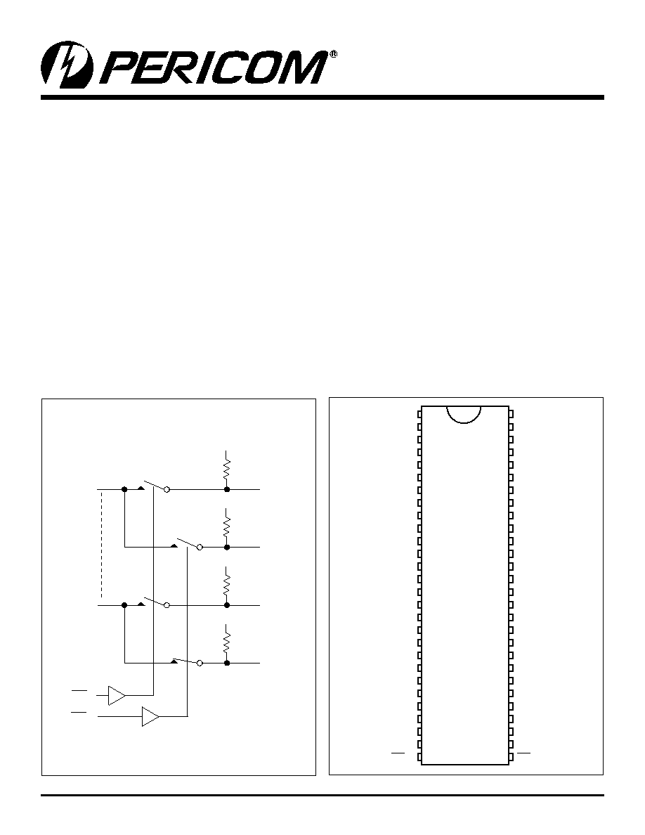
Pericom Semiconductor's PI5C32160C is a 16 to 32-bit
demultiplexer bus switch. Industry leading advantages include
a propagation delay of 250ps, resulting from 5 channel
resistance, and low I/O capacitance. A port demultiplexes to
either 1B and 2B or to both. The switch is bidirectional.
Application
Provides PCI Hot-Plugging
Block Diagram
Pin Description
Features
∑ R
ON
is 5 typical
∑ Pull-up on B1 and B2 ports
∑ Undershoot protection on A-port only: ≠1.5V
∑ Low Power: 70µA typical
∑ Industrial Operation Temperature: ≠40∫C to +85∫C
∑ Near-Zero propagation delay
∑ Switching speed: 5ns max.
∑ Channel on capacitance: 15pF max.
∑ V
CC
Operating Range: +4.5V to +5.5V
∑ ESD>2000V . . . Human Body Model
∑ >100 MHz bandwidth (or clock rate) at 20pF load capacitance
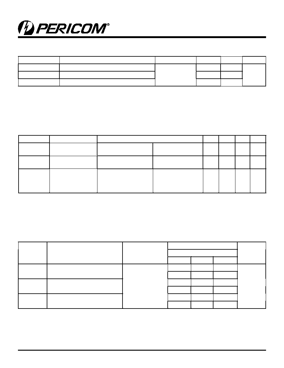
∑ Packaging (Pb-free & Green available)
- 56-pin TSSOP (A)
PI5C32160C
16-Bit to 32-Bit, DeMux PCI Hot-Plug Bus Switch
with ≠1.5V Undershoot Protection
Pullup
16B2
SEL1
16A
1A
SEL2
VBIAS2
VBIAS1
Pullup
16B1
Pullup
1B2
VBIAS2
VBIAS1
Pullup
1B1

PI5C32160C
16-Bit to 32-Bit, DeMux PCI Hot-Plug Bus Switch
with ≠1.5V Undershoot Protection
2
PS8362E 03/10/05
DC Electrical Characteristics
(Over the Operating Range, T
A
= ≠40∞C to +85∞C, V
CC
= 5V ±10%, V
BIAS
= 1.3V to V
CC
)
Parameters
Description
Test Conditions
(1)
Min.
Typ
(2)
Max.
Units
V
IH
Input HIGH Voltage
Guaranteed Logic HIGH Level
2.0
V
V
IL
Input LOW Voltage
Guaranteed Logic LOW Level
≠0.5
0.8
I
IH
Input HIGH Current
V
CC
= Max., V
IN
= V
CC
±1
µA
I
IL
Input LOW Current
V
CC
= Max., V
IN
= GND
±1
I
OZH
High Impedance Output Current A= 0V or V
CC
Max.,
V
BIAS
1 = V
BIAS
2 = V
CC
Max.
±1
I
OZL
Low Impedence Output Current
B = 0V, V
BIAS
1 = V
BIAS
2 = V
CC
Max.
0.25
5
mA
B = V
CC
max.,
V
BIAS
1 = V
BIAS
2 = V
CC
Max.
≠1.0
µA
V
IK
Clamp Diode Voltage
V
CC
= Min., I
IN
= ≠18mA
≠0.7
≠1.8
V
R
ON
Switch On-Resistance
(4)
V
CC
= Min., V
IN
= 0.0V, I
ON
= 48mA
5
8
V
CC
= Min., V
IN
= 2.4V, I
ON
= 15mA
10
15
Storage Temperature ............................................................≠65∞C to +150∞C
Ambient Temperature with Power Applied ...........................≠40∞C to +85∞C
Supply Voltage to Ground Potential (Inputs & V
CC
Only).....≠0.5V to +7.0V
Supply Voltage to Ground Potential (Outputs & D/O Only) ..≠0.5V to +7.0V
DC Input Voltage ....................................................................≠0.5V to +7.0V
DC Output Current............................................................................... 120mA
Power Dissipation ................................................................................... 0.5W
Note:
Stresses greater than those listed under MAXIMUM
RATINGS may cause permanent damage to the device.
This is a stress rating only and functional operation
of the device at these or any other conditions above those
indicated in the operational sections of this specification is
not implied. Exposure to absolute maximum rating conditions
for extended periods may affect reliability.
Maximum Ratings
(Above which the useful life may be impaired. For user guidelines, not tested.)
Truth Table
Function
SEL
1
SEL
2
N
A to
N
B
1
L
H
N
A to
N
B
2
H
L
N
A to
N
B
1
and
N
B
2
L
L
N
B
1
,
N
B
2
to V
BIAS
H
H
PI5C32160C
16-Bit to 32-Bit, DeMux PCI Hot-Plug Bus Switch
with ≠1.5V Undershoot Protection
3
PS8362E 03/10/05
Switching Characteristics over Operating Range
Parameters
Description
Test Conditions
(1)
PI5C32160C
Units
Com.
Min.
Typ.
Max.
t
PLH
t
PHL
Propagation Delay
(2,3)
A to B
C
L
= 50pF
R
L
= 500
0.25
ns
t
PZH
t
PZL
Bus Enable Time
SEL
TO
A,B
1.3
5.0
t
PHZ
t
PLZ
Bus Disable Time
SEL to A,B
0.5
5.0
Power Supply Characteristics
Parameters
Description
Test Conditions
(1)
Min.
Typ
(2)
Max. Units
I
CC
Quiescent Power
Supply Current
V
CC
= Max.
V
IN
= GND or V
CC
70
200
µA
I
CC
Supply Current per
Input @ TTL HIGH
V
CC
= Max.
V
IN
= 3.4V
(3)
other pin=V
CC
or GND
2.5
mA
I
CCD
Supply Current per
Input per MHz
(4)
V
CC
= Max.,
A and B Pins Open
Control Input Toggling
50% Duty Cycle
0.25
mA/
MHz
Notes:
1. For Max. or Min. conditions, use appropriate value specified under Electrical Characteristics for the applicable device.
2. Typical values are at V
CC
= 5.0V, +25∞C ambient.
3. Per TTL driven input (V
IN
= 3.4V, control inputs only); A and B pins do not contribute to I
CC
.
4. This current applies to the control inputs only and represent the current required to switch internal capacitance at the specified frequency.
The A and B inputs generate no significant AC or DC currents as they transition. This parameter is not tested, but is guaranteed by design.
5. Values for these conditions are examples of the I
CC
formula. These limits are guaranteed but not tested.
Notes:
1. See test circuit and waveforms.
2. This parameter is guaranteed but not tested on Propagation Delays.
3. The bus switch contributes no propagational delay other than the RC delay of the On-Resistance of the switch and the load capacitance. The
time constant for the switch alone is of the order of 0.25ns for 50pF load. Since this time constant is much smaller than the rise/fall times of
typical driving signals, it adds very little propagational delay to the system. Propagational delay of the bus switch when used in a system is
determined by the driving circuit on the driving side of the switch and its interaction with the load on the driven side.
Capacitance
(T
A
= 25∞C, f = 1 MHz)
Parameters
(5)
Description
Test Conditions
Typ.
Max.
Units
C
IN
Input Capacitance
V
IN
= 0V
3.5
pF
C
OFF
A/B Capacitance, Switch Off
6.5
C
ON
A/B Capacitance, Switch On
13.5
Notes:
1. For Max. or Min. conditions, use appropriate value specified under Electrical Characteristics for the applicable device type.
2. Typical values are at V
CC
= 5.0V, T
A
= 25∞C ambient and maximum loading.
3. Not more than one output should be shorted at one time. Duration of the test should not exceed one second.
4. Measured by the voltage drop between A and B pins at indicated current through the switch. On-Resistance is determined by the lower of the
voltages on the two (A & B) pins.
5. This parameter is determined by device characterization but is not production tested.
PI5C32160C
16-Bit to 32-Bit, DeMux PCI Hot-Plug Bus Switch
with ≠1.5V Undershoot Protection
4
PS8362E 03/10/05
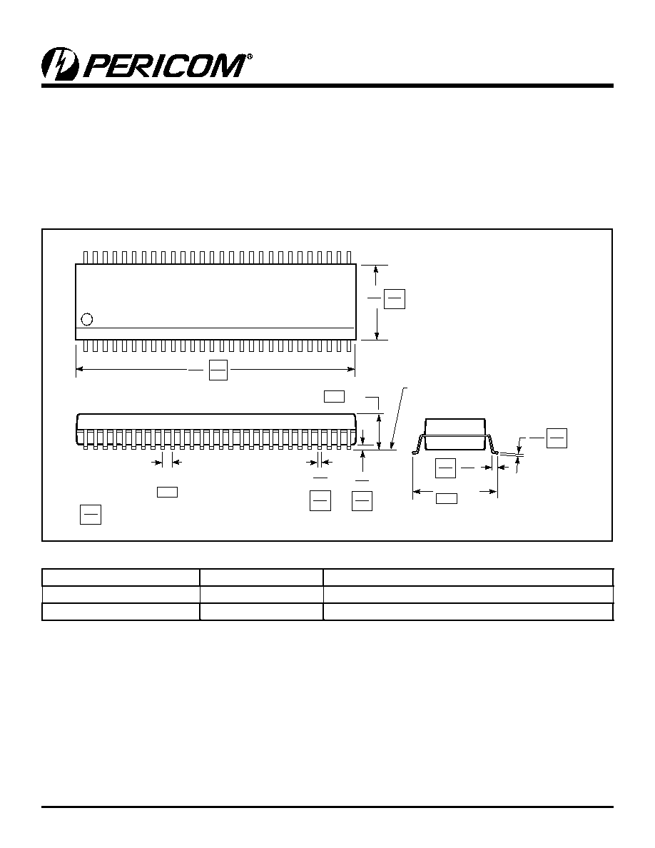
.002
.006
SEATING PLANE
.007
.011
.004
.008
1
56
.236
.244
0.50
0.17
0.27
0.05
0.15
0.09
0.20
X.XX
X.XX
DENOTES DIMENSIONS
IN MILLIMETERS
.018
.030
0.45
0.75
.047
Max.
1.20
6.0
6.2
.547
.555
13.9
14.1
.319
8.1
.0197
BSC
BSC
Pericom Semiconductor Corporation ∑ 1-800-435-2336 ∑ www.pericom.com
Packaging Mechanical: 56-pin TSSOP (A)
Applications Information
Logic Inputs
The logic control inputs can be driven up to +5.5V regardless of the supply voltage. For example, given a +5.0V supply, IN may be
driven low to 0V and high to 5.5V. Driving IN Rail-to-RailÆ minimizes power consumption. Proper power-supply sequencing is
recommended for all CMOS devices. Always apply V
CC
before applying Vbias and signals to the input/output pins.
Rail-to-Rail is a registered trademark of Nippon Motorola, Ltd
Ordering Information
Ordering Code
Package Code
Package Description
PI5C32160CA
A
56-pin 240-mil wide, TSSOP
PI5C32160CAE
A
Pb-free & Green, 56-pin 240-mil wide, TSSOP
Notes:
1. Thermal characteristics can be found on the company web site at www.pericom.com/packaging/