149
PS8136 08/20/97
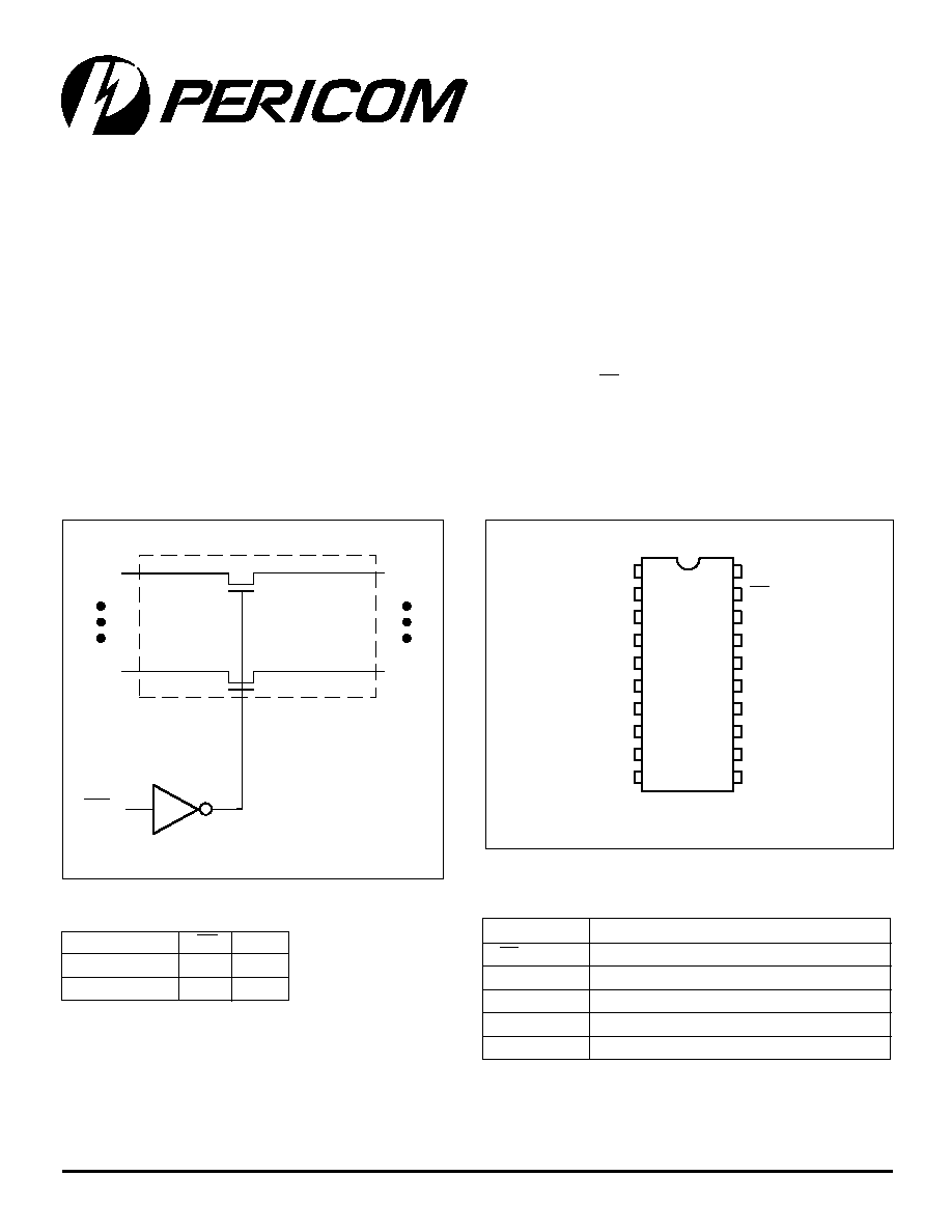
Function
BE
A
0≠7
Disconnect
H
Hi-Z
Connect
L
B
0≠7
Truth Table
(1)
Note:
1. H
=
High Voltage Level
L
=
Low Voltage Level
Hi-Z =
High Impedance
Logic Block Diagram
Product Pin Description
Pin Name
Description
BE
Bus Enable Input (Active LOW)
A
0
≠
7
Bus A
B
0
≠
7
Bus B
GND
Ground
V
CC
Power
Product Pin Configuration
PI5C32245
8-Bit, 2-Port Bus Switch
with 25
Series Resistor
12345678901234567890123456789012123456789012345678901234567890121234567890123456789012345678901212345678901234567890123456789012123456789012
12345678901234567890123456789012123456789012345678901234567890121234567890123456789012345678901212345678901234567890123456789012123456789012
Product Features:
∑ Near zero propagation delay
∑ 25
series resistor termination
∑ 5
switches connect inputs to outputs
∑ Direct bus connection when switches are ON
∑ Ultra Low Quiescent Power (0.2 µA Typical)
≠ Ideally suited for notebook applications
∑ Pin compatible with 74 series 245 logic devices
∑ Packages available:
≠ 20-pin 150 mil wide plastic QSOP (Q)
Product Description:
Pericom Semiconductor's PI5C series of logic circuits are
produced in the Company's advanced 0.8 micron CMOS technology,
achieving industry leading performance.
The PI5C32245 is a 8-bit, 2-port bus switch designed with a low
ON resistance (5
) allowing inputs to be connected directly to
outputs. The bus switch creates no additional propagational delay
or additional ground bounce noise. The switches are turned ON by
the Bus Enable (BE) input signal. Pinout is compatible with
PI74FCT245T (Octal Bidirectional Transceiver). The device has a
built-in 25
resistor to reduce noise resulting from reflections, thus
eliminating the need for an external terminating resistor.
BE
A
7
A
0
B
7
B
0
V
CC
NC
1
20
BE
A
0
2
19
B
0
A
1
3
18
B
1
A
2
4
17
B
2
A
3
5
16
B
3
A
4
6
15
B
4
A
5
7
14
B
5
A
6
8
13
B
6
A
7
9
12
B
7
GND
10
11
20-PIN
Q
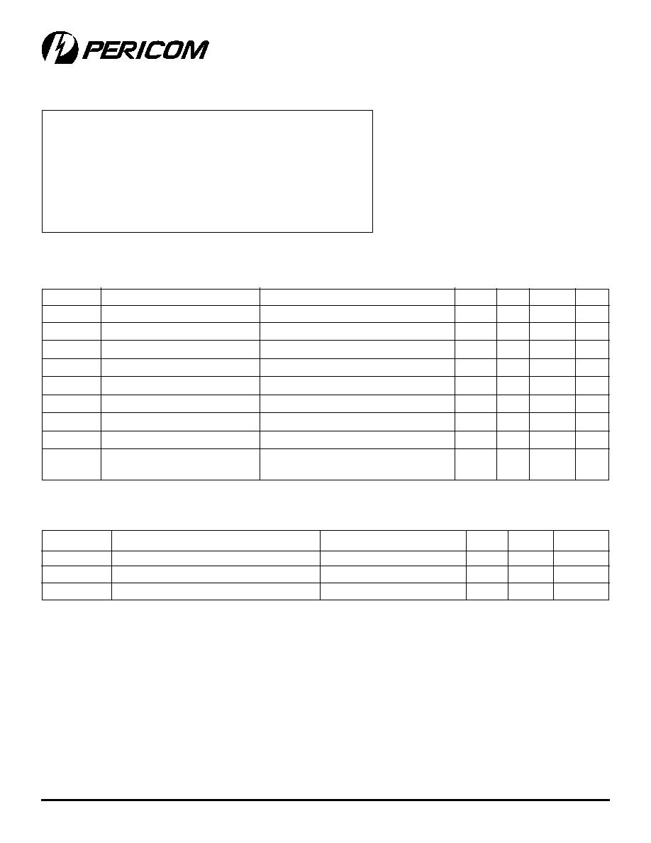
150
PS8136 08/20/97
12345678901234567890123456789012123456789012345678901234567890121234567890123456789012345678901212345678901234567890123456789012123456789012
12345678901234567890123456789012123456789012345678901234567890121234567890123456789012345678901212345678901234567890123456789012123456789012
PI5C32245
8-BIT, 2-PORT BusSwitch
with 25
Series Resistor
DC Electrical Characteristics
(Over the Operating Range, T
A
= ≠40∞C to +85∞C, V
CC
=5V ±5%)
Parameters Description
Test Conditions
(1)
Min.
Typ
(2)
Max.
Units
V
IH
Input HIGH Voltage
Guaranteed Logic HIGH Level
2.0
V
V
IL
Input LOW Voltage
Guaranteed Logic LOW Level
≠0.5
0.8
V
I
IH
Input HIGH Current
V
CC
= Max., V
IN
= V
CC
±1
µA
I
IL
Input LOW Current
V
CC
= Max., V
IN
= GND
±1
µA
I
OZH
High Impedance Output Current
0
A, B
V
CC
±1
µA
V
IK
Clamp Diode Voltage
V
CC
= Min., I
IN
= ≠18 mA
≠0.7
≠1.2
V
I
OS
Short Circuit Current
(3)
A (B) = 0V, B (A) = V
CC
100
mA
V
H
Input Hysteresis at Control Pins
150
mV
R
ON
Switch On Resistance
(4)
V
CC
= Min., V
IN
= 0.0V, I
ON
= 48 mA
28
40
V
CC
= Min., V
IN
= 2.4V, I
ON
= 15 mA
35
48
Storage Temperature ........................................................ ≠65∞C to +150∞C
Ambient Temperature with Power Applied ....................... ≠40∞C to +85∞C
Supply Voltage to Ground Potential (Inputs & Vcc Only) . ≠0.5V to +7.0V
Supply Voltage to Ground Potential (Outputs & D/O Only)≠0.5V to +7.0V
DC Input Voltage ................................................................ ≠0.5V to +7.0V
DC Output Current .......................................................................... 120 mA
Power Dissipation ................................................................................ 0.5W
Note:
Stresses greater than those listed under MAXIMUM
RATINGS may cause permanent damage to the device.
This is a stress rating only and functional operation of
the device at these or any other conditions above those
indicated in the operational sections of this specifica-
tion is not implied. Exposure to absolute maximum
rating conditions for extended periods may affect reli-
ability.
Capacitance
(T
A
= 25∞C, f = 1 MHz)
Parameters
(5)
Description
Test Conditions
Typ
Max.
Units
C
IN
Input Capacitance
V
IN
= 0V
6
pF
C
OFF
A/B Capacitance, Switch Off
V
IN
= 0V
6
pF
C
ON
A/B Capacitance, Switch On
V
IN
= 0V
8
pF
Notes:
1. For Max. or Min. conditions, use appropriate value specified under Electrical Characteristics for the applicable device type.
2. Typical values are at Vcc = 5.0V, T
A
= 25∞C ambient and maximum loading.
3. Not more than one output should be shorted at one time. Duration of the test should not exceed one second.
4. Measured by the voltage drop between A and B pin at indicated current through the switch. ON resistance is determined by the
lower of the voltages on the two (A,B) pins.
5. This parameter is determined by device characterization but is not production tested.
Maximum Ratings
(Above which the useful life may be impaired. For user guidelines, not tested.)
PI5C32245
8-BIT, 2-PORT BusSwitch
with 25
Series Resistor
151
PS8136 08/20/97
12345678901234567890123456789012123456789012345678901234567890121234567890123456789012345678901212345678901234567890123456789012123456789012
12345678901234567890123456789012123456789012345678901234567890121234567890123456789012345678901212345678901234567890123456789012123456789012
1
2
3
4
5
6
7
8
9
10
11
12
13
14
15
Power Supply Characteristics
Parameters Description
Test Conditions
(1)
Min.
Typ
(2)
Max.
Units
I
CC
Quiescent Power
V
CC
= Max.
V
IN
= GND or V
CC
0.1
3.0
µA
Supply Current
I
CC
Supply Current per
V
CC
= Max.
V
IN
= 3.4V
(3)
2.5
mA
Input @ TTL HIGH
I
CCD
Supply Current per
V
CC
= Max.,
0.25
mA/
Input per MHz
(4)
A and B Pins Open
MHz
BE = GND
Control Input Toggling
50% Duty Cycle
Notes:
1. For Max. or Min. conditions, use appropriate value specified under Electrical Characteristics for the applicable device.
2. Typical values are at Vcc = 5.0V, +25∞C ambient.
3. Per TTL driven input (V
IN
= 3.4V, control inputs only); A and B pins do not contribute to Icc.
4. This current applies to the control inputs only and represent the current required to switch internal capacitance at the specified
frequency. The A and B inputs generate no significant AC or DC currents as they transition. This parameter is not tested, but is
guaranteed by design.
Switching Characteristics over Operating Range
PI5C32245
Com.
Parameters
Description
Conditions
(1)
Min.
Max. Unit
t
PLH
Propagation Delay
(2,3)
C
L
= 50 pF
1.25
ns
t
PHL
Ax to Bx, Bx to Ax
R
L
= 500
t
PZH
Bus Enable Time
1.5
7.5
ns
t
PZL
BE to Ax or Bx
t
PHZ
Bus Disable Time
1.5
5.5
ns
t
PLZ
BE to Ax or Bx
Notes:
1. See test circuit and waveforms.
2. This parameter is guaranteed but not tested on Propagation Delays.
3. The bus switch contributes no propagational delay other than the RC delay of the ON resistance of the switch and the load
capacitance. The time constant for the switch alone is of the order of 0.25 ns for 50 pF load. Since this time constant is much
smaller than the rise/fall times of typical driving signals, it adds very little propagational delay to the system. Propagational delay
of the bus switch when used in a system is determined by the driving circuit on the driving side of the switch and its interaction
with the load on the driven side.
Pericom Semiconductor Corporation
2380 Bering Drive ∑ San Jose, CA 95131 ∑ 1-800-435-2336 ∑ Fax (408) 435-1100 ∑ http://www.pericom.com