1
PS7016B 09/14/04
1
2
3
4
5
6
7
8
9
10
11
12
13
14
15
PI5C3251
8:1 Mux/DeMux BusSwitch
Features:
∑ Near-Zero propagation delay
∑ 5 switches connect inputs to outputs
∑ Direct bus connection when switches are ON
∑ Ultra Low Quiescent Power (0.2 µA Typical)
≠ Ideally suited for notebook applications
∑ Pin compatible with 74 series 251 logic devices
∑ Packaging (Pb-free & Green available):
≠ 16-pin 150-mil wide plastic QSOP (Q)
≠ 16-pin 300-mil wide plastic SOIC (S)
≠ 16-pin 150-mil wide plastic SOIC (W)
≠ 16-pin 173-mil wide plastic TSSOP (L)
Truth Table
(1)
Select
E
S
2
S
1
S
0
Y
Function
H
X
X
X
Hi-Z
Disable
L
L
L
L
I0
S2-0 = 0
L
L
L
H
I1
S2-0 = 1
L
L
H
L
I2
S2-0 = 2
L
L
H
H
I3
S2-0 = 3
L
H
L
L
I4
S2-0 = 4
L
H
L
H
I5
S2-0 = 5
L
H
H
L
I6
S2-0 = 6
L
H
H
H
I7
S2-0 = 7
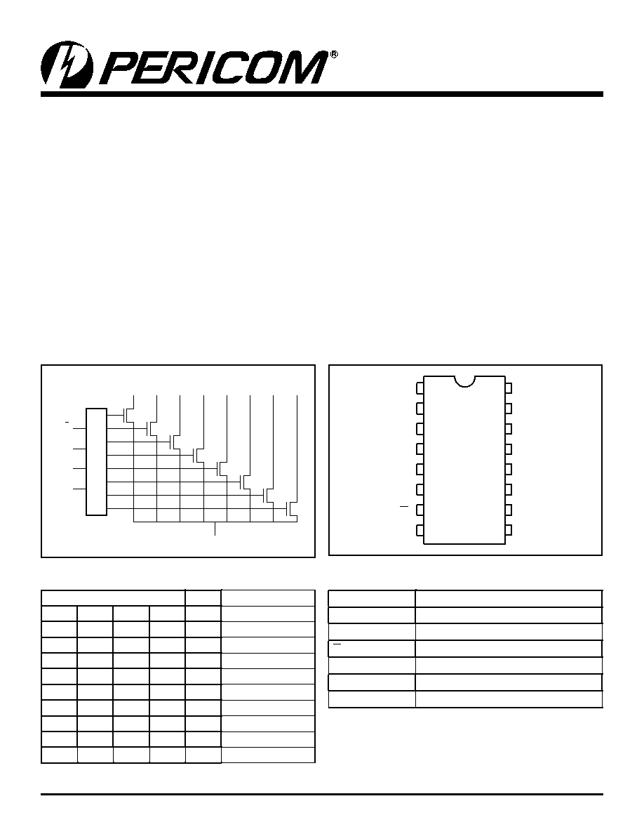
Block Diagram
Description:
Pericom Semiconductor's PI5C3251 is a Dual 8:1 Multiplexer/
demultiplexer with three-state outputs that is pinout compatible
with the PI74FCT251T, 74F251, and 74ALS/AS/LS 251. Inputs
can be connected to outputs with low on resistance (5) with no
additional ground bounce noise or propagation delay.
Pin Configuration
Pin Description
Pin Name
Description
I
0
≠
7
Data Inputs
S
0
≠
2
Select Inputs
E
Enable
Y
Data Outputs
GND
Ground
V
CC
Power
Note:
1. H = High Voltage Level, L = Low Voltage Level
E
I0
I1
I2
I3
I4
I5
I6
I7
S0
S1
S2
Y
VCC
I3
1
I4
I2
2
I5
I1
3
I6
I0
4
I7
Y
5
16
S0
NC
6
15
S1
E
7
14
S2
8
13
12
GND
11
10
9
PI5C3251
8:1 Mux/DeMux BusSwitch
2
PS7016B 09/14/04
Maximum Ratings
(Above which the useful life may be impaired. For user guidelines, not tested.)
Storage Temperature .................................................................. ≠65∞C to +150∞C
Ambient Temperature with Power Applied ................................. ≠40∞C to +85∞C
Supply Voltage to Ground Potential (Inputs & V
CC
Only)........... ≠0.5V to +7.0V
Supply Voltage to Ground Potential (Outputs & D/O Only) ........ ≠0.5V to +7.0V
DC Input Voltage .......................................................................... ≠0.5V to +7.0V
DC Output Current.....................................................................................120 mA
Power Dissipation ..........................................................................................0.5W
Note:
Stresses greater than those listed under MAXIMUM
RATINGS may cause permanent damage to the device.
This is a stress rating only and functional operation of
the device at these or any other conditions above those
indicated in the operational sections of this specifica-
tion is not implied. Exposure to absolute maximum
rating conditions for extended periods may affect
reliability.
DC Electrical Characteristics
(Over the Operating Range, T
A
= ≠40∞C to +85∞C, V
CC
=5V ±5%)
Parameters
Description
Test Conditions
(1)
Min.
Typ
(2)
Max.
Units
V
IH
Input HIGH Voltage
Guaranteed Logic HIGH Level
2.0
V
V
IL
Input LOW Voltage
Guaranteed Logic LOW Level
≠0.5
0.8
I
IH
Input HIGH Current
V
CC
= Max., V
IN
= V
CC
±1
µA
I
IL
Input LOW Current
V
CC
= Max., V
IN
= GND
±1
I
OZH
High Impedance Output Current
0 I, Y V
CC
±1
V
IK
Clamp Diode Voltage
V
CC
= Min., I
IN
= ≠18 mA
≠0.7
≠1.2
V
I
OS
Short Circuit Current
(3)
I (Y) = 0V, Y (I) = V
CC
100
mA
V
H
Input Hysteresis at Control Pins
150
mV
R
ON
Switch On-Resistance
(4)
V
CC
= Min., V
IN
= 0.0V, I
ON
= 48 mA
5
7
V
CC
= Min., V
IN
= 2.4V, I
ON
= 15 mA
10
15
Capacitance
(T
A
= 25∞C, f = 1 MHz)
Parameters
(5)
Description
Test Conditions
Typ.
Max.
Units
C
IN
Input Capacitance
V
IN
= 0V
6
pF
C
I(OFF)
I
0
- I
7
Capacitance, Switch Off
6
C
Y(OFF)
Y Capacitance, Switch Off
48
C
I(ON)
I
0
- I
7
Capacitance, Switch On
35
54
Notes:
1. For Max. or Min. conditions, use appropriate value specified under Electrical Characteristics for the applicable device type.
2. Typical values are at V
CC
= 5.0V, T
A
= 25∞C ambient and maximum loading.
3. Not more than one output should be shorted at one time. Duration of the test should not exceed one second.
4. Measured by the voltage drop between I and Y pin at indicated current through the switch. On-Resistance is determined by the lower of the
voltages on the two (I,Y) pins.
5. This parameter is determined by device characterization but is not production tested.
PI5C3251
8:1 Mux/DeMux BusSwitch
3
PS7016B 09/14/04
Power Supply Characteristics
Parameters
Description
Test Conditions
(1)
Min. Typ
(2)
Max. Units
I
CC
Quiescent Power Supply Current V
CC
= Max.
V
IN
= GND or
V
CC
0.1
3.0
µA
I
CC
Supply Current per
Input @ TTL HIGH
V
CC
= Max.
V
IN
= 3.4V
(3)
2.5
mA
I
CCD
Supply Current per
Input per MHz
(4)
V
CC
= Max.,
I and Y Pins Open
E = GND
Control Input Toggling
50% Duty Cycle
0.25
mA/
MHz
Notes:
1. For Max. or Min. conditions, use appropriate value specified under Electrical Characteristics for the applicable device.
2. Typical values are at Vcc = 5.0V, +25∞C ambient.
3. Per TTL driven input (V
IN
= 3.4V, control inputs only); I and Y pins do not contribute to Icc.
4. This current applies to the control inputs only and represent the current required to switch internal capacitance at the specified frequency. The I
and Y inputs generate no significant AC or DC currents as they transition. This parameter is not tested, but is guaranteed by design.
Switching Characteristics over Operating Range
Parameters
Description
Conditions
(1)
Com.
Unit
Min.
Max.
t
IY
Propagation Delay
(2,3)
In to Y
C
L
= 50 pF
R
L
= 500
0.25
ns
t
SY
Bus Select Time
Sn to Y
0.5
6.6
t
PZH
t
PZL
Bus Enable Time
E to Y
0.5
6.0
t
PHZ
t
PLZ
Bus Disable Time
E to Y
0.5
6.0
Notes:
1. See test circuit and wave forms.
2. This parameter is guaranteed but not tested on Propagation Delays.
3. The bus switch contributes no propagational delay other than the RC delay of the On-Resistance of the switch and the load capacitance. The
time constant for the switch alone is of the order of 0.25 ns for 50 pF load. Since this time constant is much smaller than the rise/fall times of
typical driving signals, it adds very little propagational delay to the system. Propagational delay of the bus switch when used in a system is
determined by the driving circuit on the driving side of the switch and its interaction with the load on the driven side.
PI5C3251
8:1 Mux/DeMux BusSwitch
4
PS7016B 09/14/04
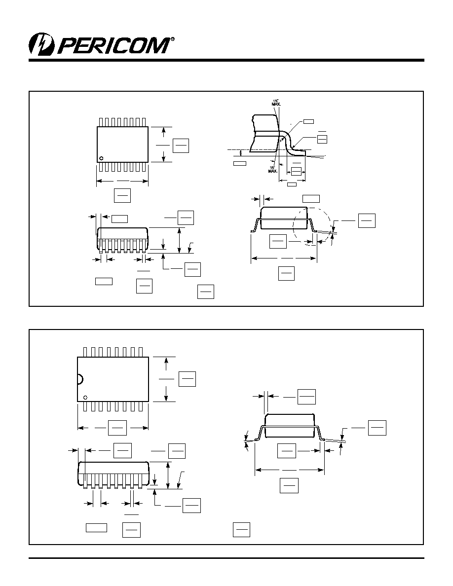
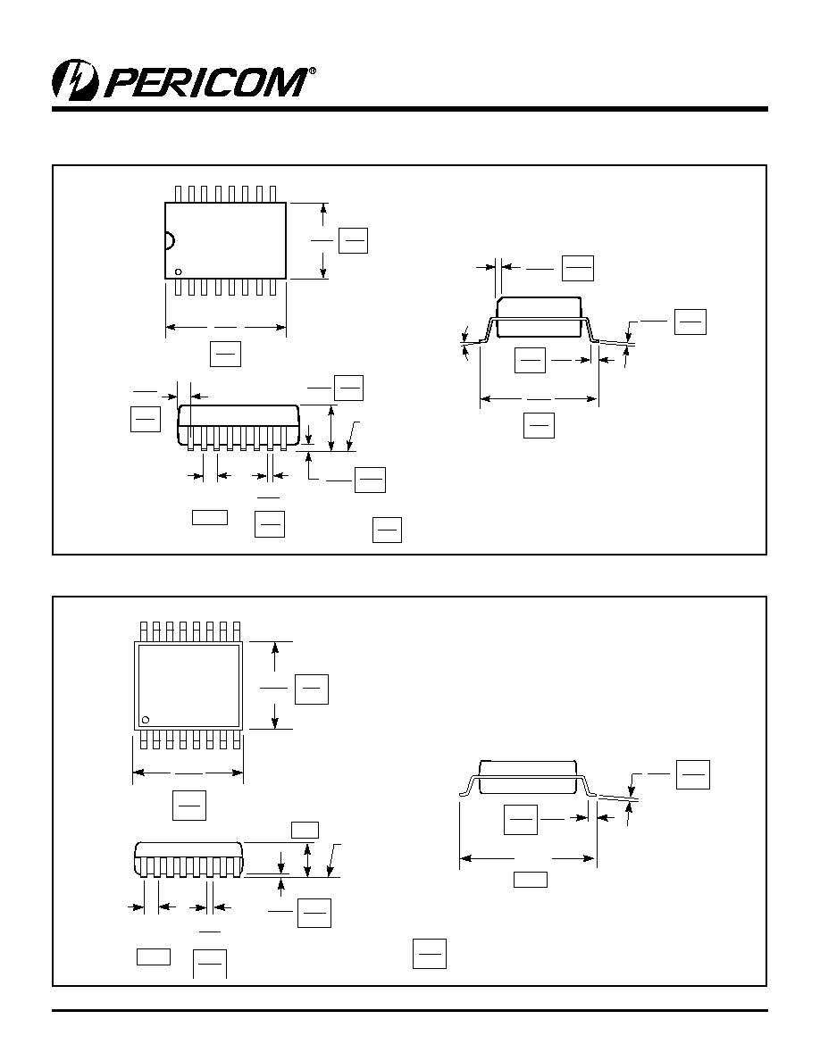
Packaging Mechanical: 16-pin QSOP (Q)
Packaging Mechanical: 16-pin SOIC (S)
SEATING
PLANE
.050
BSC
1
16
0-8∞
.2914
.2992
X.XX
X.XX
DENOTES DIMENSIONS
IN MILLIMETERS
7.40
7.60
.398
.413
10.10
10.50
1.27
.0926
.1043
2.35
2.64
.394
.419
10.00
10.65
.0040
.0118
0.10
0.30
.013
.020
.020
.030
0.33
0.51
0.508
0.762
.0091
.0125
0.254
0.737
.010
.029
x 45∞
0.23
0.32
.016
.050
0.41
1.27
.189
.197
.053
.069
.004
.010
SEATING
PLANE
.025
BSC
.007
.010
.228
.244
1
16
.150
.157
.016
.050
X.XX
X.XX
DENOTES DIMENSIONS IN MILLIMETERS
0.635
4.80
5.00
1.35
1.75
5.79
6.19
0.101
0.254
.008
.012
0.203
0.305
3.81
3.99
0.178
0.254
0.38
0.41
1.27
.008
0.203
.015 x 45
∞
REF
Detail A
Detail A
.008
0.20
MIN.
Guage Plane
.010
0.254
.041
1.04
REF
.016
.035
0.41
0.89
0∞-6∞
.008
.013
0.20
0.33
PI5C3251
8:1 Mux/DeMux BusSwitch
5
PS7016B 09/14/04
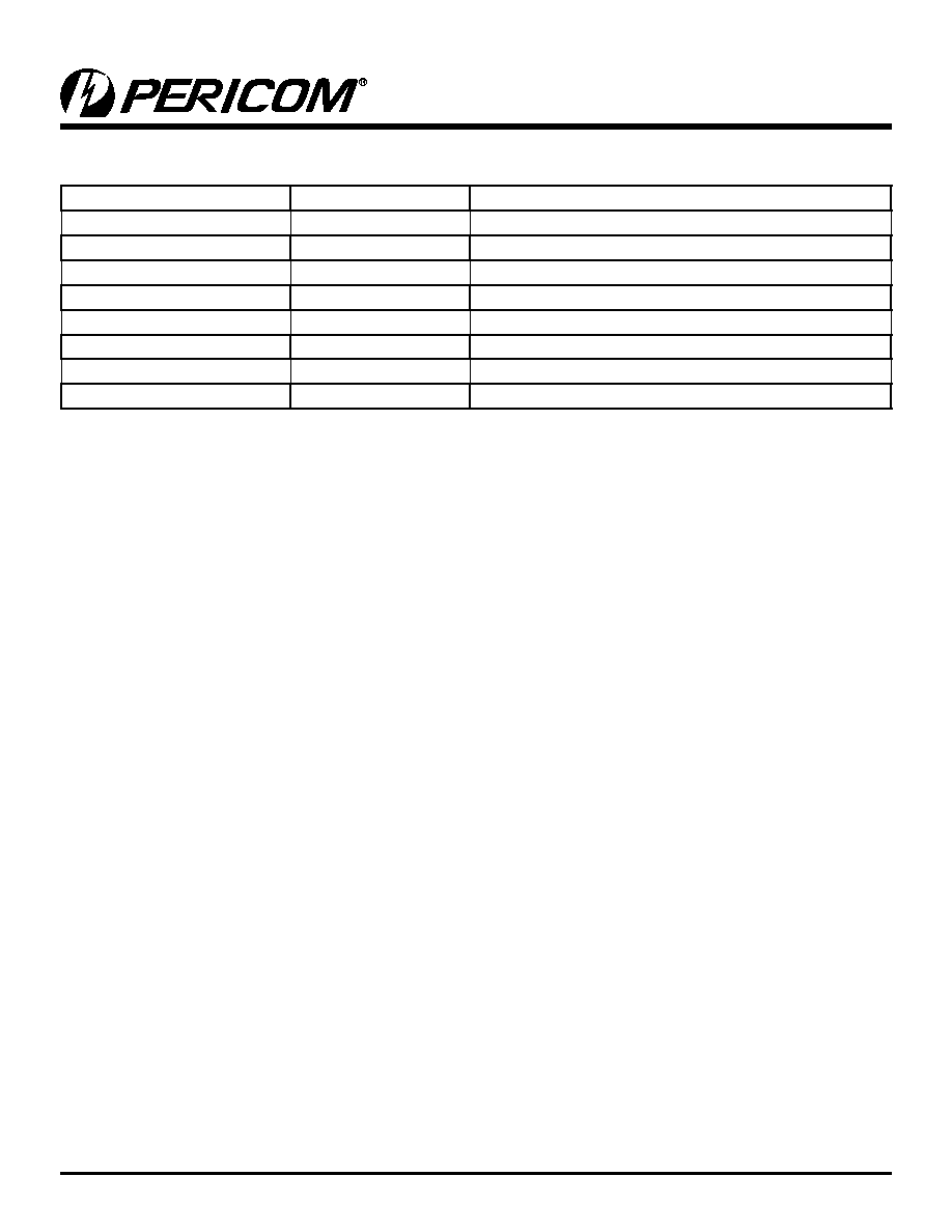
Packaging Mechanical: 16-pin SOIC (W)
Packaging Mechanical: 16-pin TSSOP (L)
.193
.201
.047
max.
.002
.006
SEATING
PLANE
.0256
BSC
.018
.030
.004
.008
.252
BSC
1
16
.169
.177
X.XX
X.XX
DENOTES CONTROLLING
DIMENSIONS IN MILLIMETERS
0.05
0.15
6.4
0.45
0.75
0.09
0.20
4.3
4.5
1.20
4.9
5.1
0.65
0.19
0.30
.007
.012
SEATING PLANE
.050
BSC
1
16
0-8∞
.149
.157
X.XX
X.XX
DENOTES DIMENSIONS
IN MILLIMETERS
3.78
3.99
.386
.393
9.80
10.00
1.27
.053
.068
1.35
1.75
.2284
.2440
5.80
6.20
.0040
.0098
0.10
0.25
.013
.020
.0155
.0260
0.330
0.508
0.393
0.660
.0075
.0098
0.25
0.50
.0099
.0196
x 45∞
0.19
0.25
.016
.050
0.41
1.27
REF
PI5C3251
8:1 Mux/DeMux BusSwitch
6
PS7016B 09/14/04
Pericom Semiconductor Corporation ∑ 1-800-435-2336 ∑ www.pericom.com
Ordering Information
Ordering Code
Package Code
Package Description
PI5C3251Q
Q
16-pin 150-mil wide QSOP
PI5C3251QE
Q
Pb-free & Green, 16-pin 150-mil wide QSOP
PI5C3251S
S
16-pin 300-mil wide SOIC
PI5C3251SE
S
Pb-free & Green, 16-pin 300-mil wide SOIC
PI5C3251W
W
16-pin 150-mil wide SOIC
PI5C3251WE
W
Pb-free & Green, 16-pin 150-mil wide SOIC
PI5C3251L
L
16-pin 173-mil wide TSSOP
PI5C3251LE
L
Pb-free & Green, 16-pin 173-mil wide TSSOP
Notes:
1. Thermal characteristics can be found on the company web site at www.pericom.com/packaging/