
1
PS8367D 10/14/04
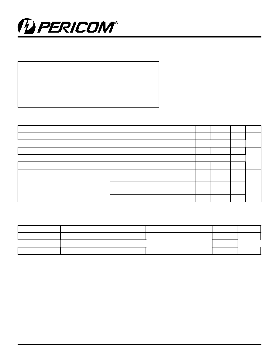
Description
Pericom Semiconductor's PI5C3303 is a single 2:1 Mux/DeMux
digital switch designed with a fast enable. When enabled using the
Bus Enable (BE) pin, the "A" or "B" pin is directly connected to
the "C" pin. The bus switch introduces no additional propagation
delay or additional ground bounce noise.
The PI5C3303 device has an active HIGH enable.
Features
∑ Near-Zero propagation delay
∑ 5 switches connect inputs to outputs
∑ Direct bus connection when switches are ON
∑ Ultra Low Quiescent Power (0.1µA Typical)
≠ Ideally suited for notebook applications
∑ Packaging (Pb-free & Green available):
≠ 6-pin plastic S0T-23 (T)
Block Diagram
Pin Configuration
A
C
B
BE
PI5C3303
SOTiny
TM
2:1 Mux/DeMux Bus Switch
Truth Table
(1)
BE
A
B
C
Function
L
C
X
A
Connect A & C
H
X
C
B
Connect B & C
Pin Description
Pin Name
Description
BE
Switch Enable
A
Bus A at pin 6
B
Bus B at pin 4
C
Bus C at pin 5
V
CC
Power
GND
Ground
Notes:
1. H = High Voltage Level
L = Low Voltage Level
X = Don't Care
2. A = I/O at pin 6
B = I/O at pin 4
C = I/O at pin 5
2
PS8367D 10/14/04
PI5C3303
SOTiny
TM
2:1 Mux/DeMux Bus Switch
Storage Temperature ..........................................................≠65∞C to +150∞C
Ambient Temperature with Power Applied .........................≠40∞C to +85∞C
Supply Voltage to Ground Potential......................................≠0.5V to +7.0V
DC Input Voltage ..................................................................≠0.5V to +7.0V
DC Output Current.............................................................................120mA
Power Dissipation .................................................................................0.5W
Note: Stresses greater than those listed under MAXI-
MUM RATINGS may cause permanent damage to
the device. This is a stress rating only and functional
operation of the device at these or any other conditions
above those indicated in the operational sections of this
specification is not implied. Exposure to absolute max-
imum rating conditions for extended periods may affect
reliability.
Maximum Ratings
(Above which the useful life may be impaired. For user guidelines, not tested.)
DC Electrical Characteristics
(Over the Operating Range, T
A
= ≠40∞C to +85∞C, V
CC
= 5V ± 10%)
Parameters
Description
Test Conditions
(1)
Min.
Typ.
(2)
Max. Units
V
IH
Input HIGH Voltage
Guaranteed Logic HIGH Level
2.0
V
V
IL
Input LOW Voltage
Guaranteed Logic LOW Level
≠0.5
0.8
I
IH
Input HIGH Current
V
CC
= Max., V
IN
= V
CC
±1
µA
I
IL
Input LOW Current
V
CC
= Max., V
IN
= GND
±1
I
OZ
High Impedence Output Current V
CC
= Max., V
OUT
= 0V or V
CC
±1
R
ON
Switch On-Resistance
(3)
V
CC
= 4V, V
IN
= 2.4V,
I
ON
= -15mA
10
20
V
CC
= 4.5V, V
IN
= 0V,
I
ON
= 30mA or 64mA
4
7
V
CC
= 4.5V, V
IN
= 2.4V, I
ON
= -15mA
7
15
Capacitance
(T
A
= 25∞C, f = 1 MHz)
Parameters(4)
Description
Test Conditions
Type
(4)
Units
C
IN
Input Capacitance
V
IN
= 0V
3
pF
C
OFF
A/B Capacitance, Switch Off
5
C
ON
A/B Capacitance, Switch On
12
Notes:
1. For Max. or Min. conditions, use appropriate value specified under Electrical Characteristics for the applicable device type.
2. Typical values are at V
CC
= 5.0V, T
A
= 25∞C ambient and maximum loading.
3. Measured by the voltage drop between A and B pin at indicated current through the switch. On-Resistance is determined by the lower of the
voltages on the two (A, B) pins.
4. This parameter is determined by device characterization but is not production tested.
3
PS8367D 10/14/04
PI5C3303
SOTiny
TM
2:1 Mux/DeMux Bus Switch
Power Supply Characteristics
Parameters
Description
Test Conditions
(1)
Min.
Typ.
(2)
Max.
Units
I
CC
Quiescent Power Supply Current
V
CC
= Max.
V
IN
= GND or V
CC
0.1
3.0
µA
I
CC
Supply Current per Input @ TTL
HIGH
V
CC
= Max.
V
IN
= 3.4V
(3)
2.5
mA
Switching Characteristics over Operating Range
Parameters
Description
Test Conditions
(3)
V
CC
= 4.5V
V
CC
= 4V
Units
Min.
Max.
Min.
Max.
t
PLH
t
PHL
Propogation Delay
(1, 2)
A to B, B to A
C
L
= 50pF
R
L
= 500
--
0.25
0.25
ns
t
PZH
t
PZL
Bus Enable Time
1.0
4.9
5.5
t
PHZ
t
PLZ
Bus Disable Time
1.0
4.2
4.5
Notes:
1. For Max. or Min. conditions, use appropriate value specified under Electrical Characteristics for the applicable device.
2. Typical values are at V
CC
= 5.0V, +25∞C ambient.
3. Per TTL driven input (V
IN
= 3.4V, control inputs only); A and B pins do not contribute to I
CC
.
Notes:
1. This parameter is guaranteed but not tested on Propagation Delays.
2. The bus switch contributes no propagational delay other than the RC delay of the On-Resistance of the switch and the load capacitance. The
time constant for the switch alone is of the order of 0.25ns for 50pF load. Since his time constant is much smaller than the rise/fall times of
typical driving signals, it adds very little propagational delay to the system. Propagational delay of the bus switch when used in a system is
determined by the driving circuit on the driving side of the switch and its interaction with the load on the driven side.
3. See test circuit and waveforms.

4
PS8367D 10/14/04
PI5C3303
SOTiny
TM
2:1 Mux/DeMux Bus Switch
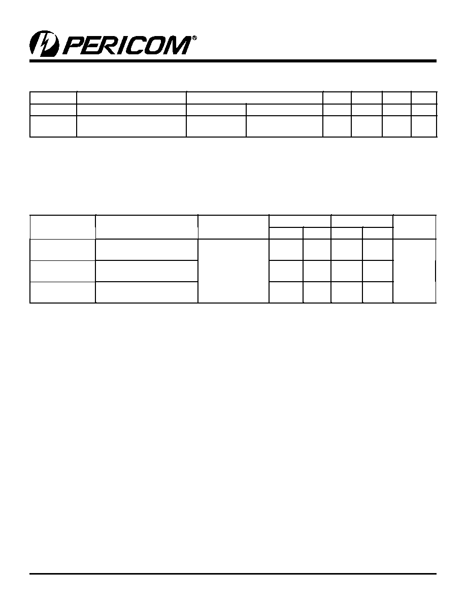
Test Circuit
Enable and Disable Timing
Switch Positions
Test
Switch
Open Drain
Disable LOW
Enable LOW
7V
All Other Inputs
Open
Notes:
1. C
L
= Load Capacitance: inlcudes jig and proble capacitance.
R
T
= Termination Resistance: should be equal to the Z
OUT
of the
Pulse Generator.
t
PLZ
1.5V
3V
3V
0V
1.5V
3V
1.5V
0V
t
PHZ
t
PZL
t
PZH
Output
Output
Normally
High
0.3V
VOL
VOH
0.3V
0V
Enable
Disable
Control
Input
Switch
Notes:
1. Input Control Enable = Low; Input Control Disable = High.
2. Pulse Generator for All Pulses: Rate 1.0 MHz; Z
OUT
50; t
F
, t
R
, 2.5ns,

5
PS8367D 10/14/04
PI5C3303
SOTiny
TM
2:1 Mux/DeMux Bus Switch
Packaging Mechanical: 6-Pin Plastic SOT-23 (T)
0.102
0.118
BSC
0.60
0.000
0.005
0.00
0.15
0.014
0.019
0.35
0.50
1.50
1.75
0.059
0.068
0.10
0.023
0.004
1.45MAX.
SEATING
PLANE
0.057
0∫ - 10∫
1.90
0.075
0.037
BSC
2.60
3.00
0.95
0.110
0.118
2.80
3.00
X.XX
X.XX
Datum "A"
DENOTES DIMENSIONS
IN MILLIMETERS
2
5
3
6
4
Ordering Information
Ordering Code
Package Code
Package Description
Top Mark
PI5C3303TX
T
6-Pin Plastic SOT-23
ZX
PI5C3303TEX
T
Pb-free & Green, 6-Pin Plastic SOT-23
ZX
Pericom Semiconductor Corporation ∑ 1-800-435-2336 ∑ www.pericom.com
Notes:
1. Thermal characteristics can be found on the company web site at www.pericom.com/packaging/
2. X = Tape and Reel