1
PS8144C 01/11/01
Product Description
Pericom Semiconductor's PI5C series of logic circuits are produced
using the Company's advanced submicron CMOS technology,
achieving industry leading speed grades.
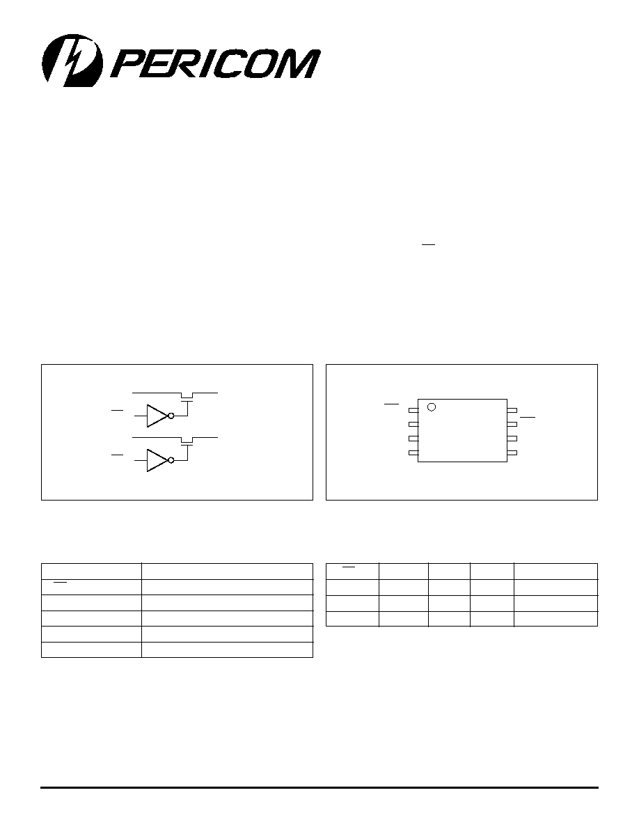
The PI5C3306 is a 2-bit bus switch designed with two 5-ohm bus
switches with fast individual enables. When enabled via the
associated Bus Enable (BE) pin, the "A" pin is directly connected to
the "B" pin for that particular gate. The bus switch introduces no
additional propagation delay or additional ground bounce noise.
The PI5C3306 device has active LOW enables.
12345678901234567890123456789012123456789012345678901234567890121234567890123456789012345678901212345678901234567890123456789012123456789012
12345678901234567890123456789012123456789012345678901234567890121234567890123456789012345678901212345678901234567890123456789012123456789012
PI5C3306
2-Bit Bus Switch with
Active Low Enables
Product Features
∑ Near zero propagation delay
∑ 5-Ohm switches connect inputs to outputs
∑ Direct bus connection when switches are ON
∑ Ultra Low Quiescent Power (0.2µA Typical)
≠ Ideally suited for notebook applications
∑ Packages available:
≠ 8-pin 173 mil wide plastic TSSOP (L)
≠ 8-pin 118 mil wide plastic MSOP (U)
Logic Block Diagram
BE1
A1
B1
BE2
A2
B2
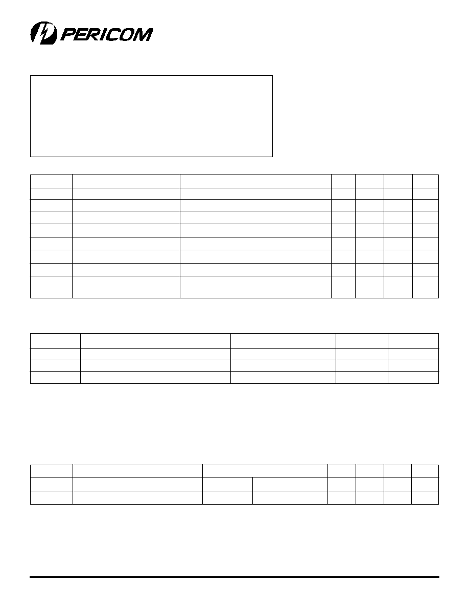
Product Pin Configuration
Product Pin Description
Pin Name
Description
BEn
Switch Enable
A2-A1
Bus A
B2-B1
Bus B
Vcc
Power
GND
Ground
BEn
An
Bn
Vcc
Function
X*
Hi-Z
Hi-Z
GND
Disconnect
H
Hi-Z
Hi-Z
Vcc
Disconnect
L
Bn
An
Vcc
Connect
Truth Table
(1)
Notes:
1. H
= High Voltage Level, L = Low Voltage Level
Hi-Z = High Impedance, X = Don't Care
* A pull-up resistor should be provided for power-up protection.
1
2
3
4
8
7
6
5
Vcc
BE2
B2
A2
BE1
A1
B1
GND
8-Pin
L, U
2
PS8144C 01/11/01
12345678901234567890123456789012123456789012345678901234567890121234567890123456789012345678901212345678901234567890123456789012123456789012
PI5C3306
2-Bit Bus Switch with Active Low Enables
Capacitance
(T
A
= 25∞C, f = 1 MHz)
Parameters
(4)
Description
Test Conditions
Typ
Units
C
IN
Input Capacitance
V
IN
= 0V
3
pF
C
OFF
A/B Capacitance, Switch Off
V
IN
= 0V
5
pF
C
ON
A/B Capacitance, Switch On
V
IN
= 0V
10
pF
Parameters
Description
Test Conditions
(1)
Min.
Typ
(2)
Max.
Units
V
IH
Input HIGH Voltage
Guaranteed Logic HIGH Level
2.0
V
V
IL
Input LOW Voltage
Guaranteed Logic LOW Level
≠0.5
0.8
V
I
IH
Input HIGH Current
V
CC
= Max., V
IN
= V
CC
±1
µA
I
IL
Input LOW Current
V
CC
= Max., V
IN
= GND
±1
µA
I
OZH
High Impedance Output Current
0
A, B
V
CC
±1
µA
I
OZL
Low Impedance Output Current
0
A, B
V
CC
±1
mA
V
H
Input Hysteresis at Control Pins
300
mV
R
ON
Switch On Resistance
(3)
V
CC
= 4.5V, V
IN
= 0.0V, I
ON
= 30mA or 64mA
5
7
V
CC
= 4.5V, V
IN
= 2.4V, I
ON
= 15mA
10
15
Storage Temperature .......................................................... ≠65∞C to +150∞C
Ambient Temperature with Power Applied ..........................≠40∞C to +85∞C
Supply Voltage to Ground Potential (Inputs & Vcc Only) .... ≠0.5V to +7.0V
Supply Voltage to Ground Potential (Outputs & D/O Only) . ≠0.5V to +7.0V
DC Input Voltage ................................................................... ≠0.5V to +7.0V
DC Output Current ............................................................................ 120mA
Power Dissipation ................................................................................. 0.5W
Note:
Stresses greater than those listed under MAXIMUM
RATINGS may cause permanent damage to the
device. This is a stress rating only and functional
operation of the device at these or any other condi-
tions above those indicated in the operational sec-
tions of this specification is not implied. Exposure to
absolute maximum rating conditions for extended
periods may affect reliability.
Notes:
1. For Max. or Min. conditions, use appropriate value specified under Electrical Characteristics for the applicable device type.
2. Typical values are at V
CC
= 5.0V, T
A
= 25∞C ambient and maximum loading.
3. Measured by the voltage drop between A and B pin at indicated current through the switch. ON resistance is determined
by the lower of the voltages on the two (A, B) pins.
4. This parameter is determined by device characterization but is not production tested.
Power Supply Characteristics
Parameters Description
Test Conditions
(1)
Min.
Typ
(2)
Max.
Units
I
CC
Quiescent Power Supply Current
V
CC
= Max.
V
IN
= GND or V
CC
0.1
3.0
µA
I
CC
Supply Current per Input @ TTL HIGH
V
CC
= Max.
V
IN
= 3.4V
(3)
2.5
mA
Notes:
1. For Max. or Min. conditions, use appropriate value specified under Electrical Characteristics for the applicable device.
2. Typical values are at V
CC
= 5.0V, +25∞C ambient.
3. Per TTL driven input (V
IN
= 3.4V, control inputs only); A and B pins do not contribute to I
CC
.
Maximum Ratings
(Above which the useful life may be impaired. For user guidelines, not tested.)
DC Electrical Characteristics
(Over the Operating Range, T
A
= ≠40∞C to +85∞C, V
CC
= 4V to 5.5V)
PI5C3306
2-Bit Bus Switch with Active Low Enables
3
PS8144C 01/11/01
12345678901234567890123456789012123456789012345678901234567890121234567890123456789012345678901212345678901234567890123456789012123456789012
1
2
3
4
5
6
7
8
9
10
11
12
13
14
15
PI5C3306 Switching Characteristics over Operating Range
Notes:
1. See test circuit and waveforms.
2. This parameter is guaranteed but not tested on Propagation Delays.
3. The bus switch contributes no propagational delay other than the RC delay of the ON resistance of the switch and the load
capacitance. The time constant for the switch alone is of the order of 0.25ns for 50pF load. Since this time constant is much smaller
than the rise/fall times of typical driving signals, it adds very little propagational delay to the system. Propagational delay of the
bus switch when used in a system is determined by the driving circuit on the driving side of the switch and its interaction with the
load on the driven side.
Pericom Semiconductor Corporation
2380 Bering Drive ∑ San Jose, CA 95131 ∑ 1-800-435-2336 ∑ Fax (408) 435-1100 ∑ http://www.pericom.com
t
r
a
P
e
g
a
k
c
a
P
-
n
i
P
e
r
u
t
a
r
e
p
m
e
T
L
6
0
3
3
C
5
I
P
)
L
(
P
O
S
S
T
-
8
C
∞
5
8
+
o
t
C
∞
0
4
≠
X
U
6
0
3
3
C
5
I
P
)
U
(
P
O
S
M
-
8
Ordering Information
s
r
e
t
e
m
a
r
a
P
n
o
i
t
p
i
r
c
s
e
D
s
n
o
i
t
i
d
n
o
C
)
1
(
6
0
3
3
C
3
I
P
s
t
i
n
U
V
C
C
%
0
1
±
V
5
=
V
C
C
V
4
=
.
n
i
M
.
x
a
M
.
n
i
M
.
x
a
M
t
H
L
P
t
L
H
P
y
a
l
e
D
n
o
i
t
a
g
o
p
o
r
P
)
3
,
2
(
A
o
t
B
,
B
o
t
A
C
L
F
p
0
5
=
R
L
0
0
5
=
--
5
2
.
0
5
2
.
0
s
n
t
H
Z
P
t
L
Z
P
e
m
i
T
e
l
b
a
n
E
s
u
B
0
.
1
9
.
4
5
.
5
t
Z
H
P
t
Z
L
P
e
m
i
T
e
l
b
a
s
i
D
s
u
B
0
.
1
2
.
4
5
.
4