 | –≠–ª–µ–∫—Ç—Ä–æ–Ω–Ω—ã–π –∫–æ–º–ø–æ–Ω–µ–Ω—Ç: PI5L100WE | –°–∫–∞—á–∞—Ç—å:  PDF PDF  ZIP ZIP |
1
PS7031F 09/17/04
e
m
a
N
n
i
P
n
o
i
t
p
i
r
c
s
e
D
n
D
I
-
n
A
I
s
t
u
p
n
I
a
t
a
D
S
s
t
u
p
n
I
t
c
e
l
e
S
E
e
l
b
a
n
E
D
Y
-
A
Y
s
t
u
p
t
u
O
a
t
a
D
D
N
G
d
n
u
o
r
G
V
C
C
r
e
w
o
P
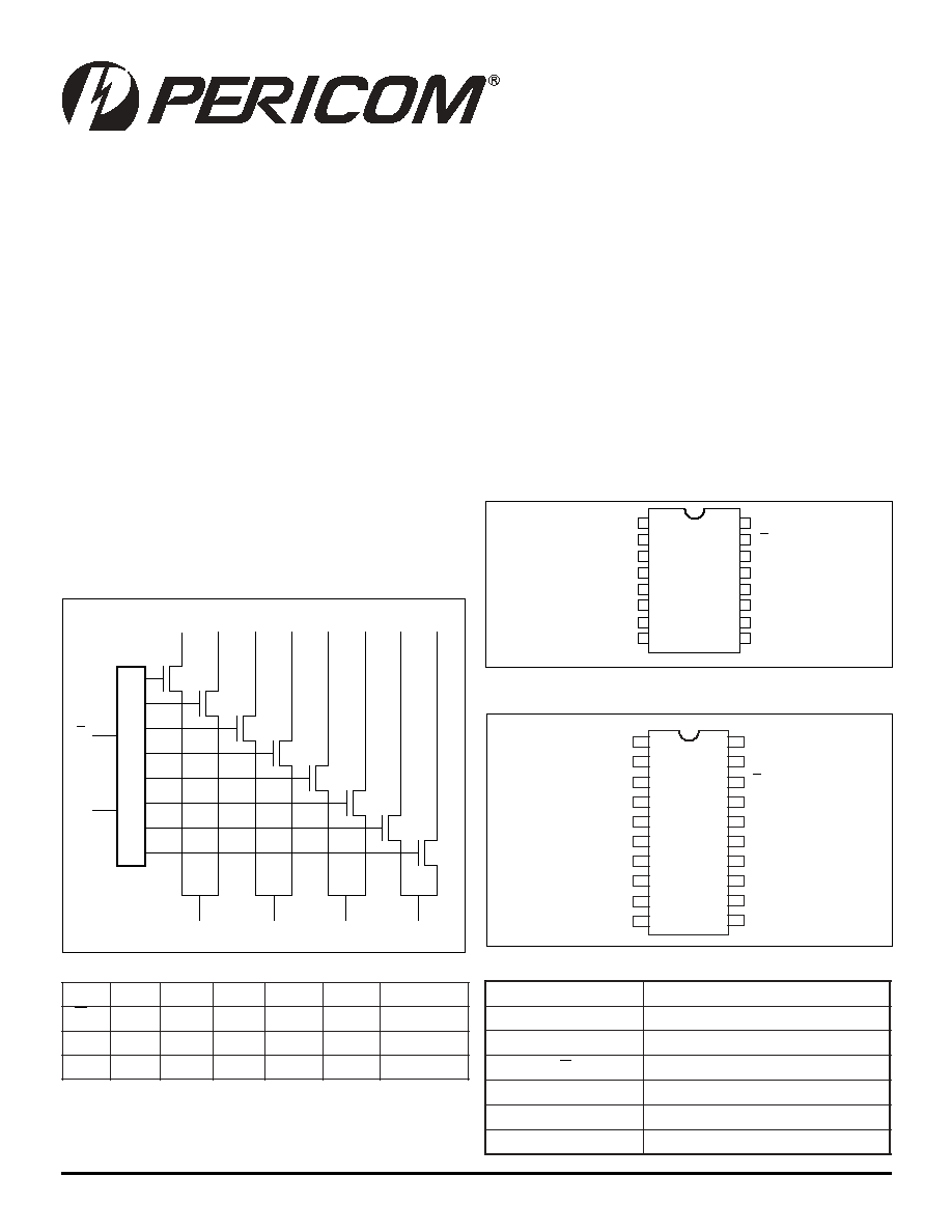
Block Diagram
12345678901234567890123456789012123456789012345678901234567890121234567890123456789012345678901212345678901234567890123456789012123456789012
12345678901234567890123456789012123456789012345678901234567890121234567890123456789012345678901212345678901234567890123456789012123456789012
16-Pin Configuration
Truth Table
(1)
Note:
1. H = High Voltage Level
L = Low Voltage Level
Product Pin Description
Wide Bandwidth
Low Voltage LanSwitch
Quad 2:1 Mux/Demux
Features
∑ Replaces mechanical relays
∑ High-performance, low-cost solution for switching
between different LAN signals
∑ Ultra-low quiescent power (0.1 µA typical)
∑ Low crosstalk: ≠40 dB @ 30 Mbps
∑ Low insertion loss or On-Resistance: 3ohms typical
∑ Single extended supply operation up to 6.2V ± 5%
∑ Off isolation: ≠30 dB @ 30 Mbps
∑ Wide bandwidth data rates > 200 Mbps
∑ Packages (Pb-free & Green available):
≠ 16-pin 150-mil wide plastic SOIC (W)
≠ 16-pin 150-mil wide plastic QSOP (Q)
≠ 20-pin 173-mil wide plastic TSSOP (L)
20-Pin Configuration
E
IA0
IA1
IB0
IB1
IC0
IC1
ID0
ID1
S
YA
YB
YC
YD
V
CC
1
S
16
E
2
IA0
15
ID0
3
IA1
14
ID1
4
YA
13
YD
5
IB0
12
IC0
6
IB1
11
IC1
7
YB
10
YC
8
GND
9
16-Pin
W,Q
V
CC
NC
1
E
S
2
ID
1
IA
0
3
ID
0
IA
1
4
YD
YA
5
20
IB
0
6
19
IC
0
IB
1
7
18
YC
8
17
16
GND
15
14
13
YB
9
10
NC
NC
12
11
NC
IC
1
Description
Pericom Semiconductor's PI5L100 is a Quad 2:1 multiplexer/
demultiplexer LanSwitch with three-state outputs. This device can
be used for switching between various standards, such as 10 Base-
T, 100 Base-T, 100VG-AnyLAN or Token Ring. Generally, this part
can be used to replace mechanical relays in low voltage LAN
applications that have phsical layer, unshielded twisted pair media
(UTP) with either CAT 3 or CAT 5 grade cable.
To reduce insertion loss, PI5L100 is powered by a 6.2V Zener voltage.
E
S
A
Y
B
Y
C
Y
D
Y
n
o
i
t
c
n
u
F
H
X
Z
-i
H
Z
-i
H
Z
-i
H
Z
-i
H
e
l
b
a
s
i
D
L
L
0
A
I
0
B
I
0
C
I
0
D
I
0
=
S
L
H
1
A
I
1
B
I
1
C
I
1
D
I
1
=
S
20-Pin
L
PI5L100

PI5L100
Wide-Bandwidth, Low-Voltage
LanSwitch Quad 2:1 Mux/Demux
2
PS7031F 09/17/04
12345678901234567890123456789012123456789012345678901234567890121234567890123456789012345678901212345678901234567890123456789012123456789012
12345678901234567890123456789012123456789012345678901234567890121234567890123456789012345678901212345678901234567890123456789012123456789012
Storage Temperature ........................................................ ≠65∞C to +150∞C
Ambient Temperature with Power Applied ............................ 0∞C to +70∞C
Supply Voltage to Ground Potential ................................... ≠0.5V to +7.0V
DC Input Voltage ................................................................ ≠0.5V to +7.0V
DC Output Current ......................................................................... 120 mA
Power Dissipation .............................................................................. 0.5W
Note:
Stresses greater than those listed under MAXIMUM RAT-
INGS may cause permanent damage to the device. This is a
stress rating only and functional operation of the device at these
or any other conditions above those indicated in the operational
sections of this specification is not implied. Exposure to
absolute maximum rating conditions for extended periods may
affect reliability.
DC Electrical Characteristics
(Over the Operating Range, T
A
= 0∞C to +70∞C, V
CC
= 6.2V, +5%, ≠ 2%)
Notes:
1. For Max. or Min. conditions, use appropriate value specified under Electrical Characteristics for the applicable device type.
2. Typical values are at V
CC
= 6.2V, T
A
= 25∞C ambient temperature.
3. Not more than one output should be shorted at one time. Duration of the test should not exceed one second.
4. V
ON
(min) value is at V
CC
= 6.1V, T
A
= 70∞C.
5. The expected AC V
ON
value is about 125 mV higher than the DC V
ON
value using the similar test circuit in Figure 10 with V
IN
swing from 0.0V
to 4.5V at 10 MHz sine wave.
6. The value of R
ON
of M1 is calculated with the equvalent mathematical formula of the test circuit in Figure 10.
Maximum Ratings
(Above which useful life may be impaired. For user guidelines, not tested.)
r
e
t
e
m
a
r
a
P
n
o
i
t
p
i
r
c
s
e
D
s
n
o
i
t
i
d
n
o
C
t
s
e
T
.
n
i
M
p
y
T
)
2
(
.
x
a
M
s
t
i
n
U
V
H
I
e
g
a
tl
o
V
H
G
I
H
t
u
p
n
I
l
e
v
e
L
H
G
I
H
c
i
g
o
L
d
e
e
t
n
a
r
a
u
G
0
.
2
--
--
V
V
L
I
e
g
a
tl
o
V
W
O
L
t
u
p
n
I
l
e
v
e
L
W
O
L
c
i
g
o
L
d
e
e
t
n
a
r
a
u
G
5
.
0
≠
--
8
.
0
A
µ
I
H
I
t
n
e
r
r
u
C
H
G
I
H
t
u
p
n
I
V
C
C
V
,.
x
a
M
=
N
I
V
=
C
C
--
--
1
±
I
L
I
t
n
e
r
r
u
C
W
O
L
t
u
p
n
I
V
C
C
V
,.
x
a
M
=
N
I
=
D
N
G
--
--
1
±
I
H
Z
O
t
n
e
r
r
u
C
t
u
p
t
u
O
e
c
n
a
d
e
p
m
I
h
g
i
H
0
B
,
A
V
C
C
--
--
1
±
V
V
K
I
e
g
a
tl
o
V
e
d
o
i
D
p
m
a
l
C
V
C
C
I
,.
n
i
M
=
N
I
A
m
8
1
≠
=
--
7
.
0
≠
2
.
1
≠
A
m
I
S
O
t
n
e
r
r
u
C
ti
u
c
ri
C
t
r
o
h
S
)
3
(
V
=
)
A
(
B
,
V
0
=
)
B
(
A
C
C
0
0
1
--
--
V
H
s
n
i
P
l
o
r
t
n
o
C
t
a
s
i
s
e
r
e
t
s
y
H
t
u
p
n
I
--
0
5
1
--
V
m
V
N
O
e
g
a
tl
o
V
n
O
h
c
ti
w
S
V
N
I
R
,
0
1
e
r
u
g
i
F
e
e
S
,
W
O
L
=
E
,
V
5
.
4
=
L
0
0
1
=
7
.
3
)
4
(
6
0
.
4
)
5
(
--
V
R
N
O
)
6
(
e
c
n
a
t
s
i
s
e
R
n
O
h
c
ti
w
S
1
M
V
m
o
r
f
d
e
t
a
l
u
c
l
a
C
N
O
9
1
2
.
1
1
--
R
N
O
)
7
(
e
c
n
a
t
s
i
s
e
R
n
O
h
c
ti
w
S
2
M
V
N
I
R
,
0
1
e
r
u
g
i
F
e
e
S
,
W
O
L
=
E
,
V
5
.
4
=
L
0
0
1
=
0
.
2
0
.
3
--
R
N
O
h
c
t
a
M
e
c
n
a
t
s
i
s
e
R
n
O
V
N
I
W
O
L
=
E
,
V
5
.
4
=
--
0
.
1
--
7. This parameter is determined by device characterization but is not production tested.
R
ON
(M1) =
were
with R
ON
(M2) = 3 ohms
V
IN
≠ V
ON
I
ON
I
ON
=
V
ON
R
L
+ R
ON
(M2)

PI5L100
Wide-Bandwidth, Low-Voltage
LanSwitch Quad 2:1 Mux/Demux
3
PS7031F 09/17/04
12345678901234567890123456789012123456789012345678901234567890121234567890123456789012345678901212345678901234567890123456789012123456789012
12345678901234567890123456789012123456789012345678901234567890121234567890123456789012345678901212345678901234567890123456789012123456789012
Capacitance
(T
A
= 25∞C, f = 1 MHz)
Note:
1. This parameter is determined by device characterization but is not production tested.
Notes:
1. For Max. or Min. conditions, use appropriate value specified under Electrical Characteristics for the applicable device.
2. Per TTL driven input (V
IN
= 3.4V, control inputs only); A and B pins do not contribute to I
CC
.
3. This current applies to the control inputs only and represent the current required to switch internal capacitance at the specified frequency.
The A and B inputs generate no significant AC or DC currents as they transition. This parameter is not tested, but is guaranteed by design.
Power Supply Characteristics
s
r
e
t
e
m
a
r
a
P
)
1
(
n
o
i
t
p
i
r
c
s
e
D
s
n
o
i
t
i
d
n
o
C
t
s
e
T
.
p
y
T
s
t
i
n
U
C
N
I
e
c
n
a
ti
c
a
p
a
C
t
u
p
n
I
V
N
I
V
0
=
6
F
p
C
F
F
O
f
f
O
h
c
ti
w
S
,
e
c
n
a
ti
c
a
p
a
C
B
/
A
V
N
I
V
0
=
6
C
N
O
n
O
h
c
ti
w
S
,
e
c
n
a
ti
c
a
p
a
C
B
/
A
V
N
I
V
0
=
8
s
r
e
t
e
m
a
r
a
P
)
1
(
n
o
i
t
p
i
r
c
s
e
D
s
n
o
i
t
i
d
n
o
C
t
s
e
T
.
n
i
M
.
p
y
T
.
x
a
M
s
t
i
n
U
I
C
C
t
n
e
r
r
u
C
y
l
p
p
u
S
r
e
w
o
P
t
n
e
c
s
e
i
u
Q
V
C
C
V
5
.
5
=
V
N
I
V
r
o
D
N
G
=
C
C
1
.
0
0
.
3
A
µ
I
C
C
h
g
i
H
L
T
T
@
t
u
p
n
I
r
e
p
t
n
e
r
r
u
C
y
l
p
p
u
S
V
C
C
V
5
.
5
=
V
N
I
=
V
4
.
3
)
2
(
5
.
2
A
m
I
D
C
C
z
H
M
r
e
p
t
n
e
r
r
u
C
y
l
p
p
u
S
)
3
(
V
C
C
V
5
.
5
=
n
e
p
O
s
n
i
P
t
u
p
n
I
D
N
G
=
E
g
n
il
g
g
o
T
t
u
p
n
I
l
o
r
t
n
o
C
e
l
c
y
C
y
t
u
D
%
0
5
5
2
.
0
z
H
M
/
A
µ

PI5L100
Wide-Bandwidth, Low-Voltage
LanSwitch Quad 2:1 Mux/Demux
4
PS7031F 09/17/04
12345678901234567890123456789012123456789012345678901234567890121234567890123456789012345678901212345678901234567890123456789012123456789012
12345678901234567890123456789012123456789012345678901234567890121234567890123456789012345678901212345678901234567890123456789012123456789012
s
r
e
t
e
m
a
r
a
P
n
o
i
t
p
i
r
c
s
e
D
s
n
o
i
t
i
d
n
o
C
)
1
(
0
0
1
L
5
I
P
s
t
i
n
U
.
m
o
C
.
n
i
M
.
p
y
T
.
x
a
M
t
Y
I
y
a
l
e
D
n
o
it
a
g
a
p
o
r
P
)
3
,
2
(
, I
N
Y
o
t
C
L
F
p
0
5
=
R
L
5
=
0
s
m
h
o
0
--
--
5
2
.
0
s
n
t
Y
S
Y
o
t
S
,
e
m
i
T
e
l
b
a
n
E
s
u
B
5
.
0
2
.
5
t
,
Z
H
P
t
Z
L
P
Y
o
t
E
,
e
m
i
T
e
l
b
a
s
i
D
s
u
B
5
.
0
0
.
5
t
Y
E
Y
o
t
E
,
e
m
i
T
e
l
b
a
s
i
D
s
u
B
5
.
0
8
.
4
X
K
L
A
T
)
fi
D
(
k
l
a
t
s
s
o
r
C
l
a
it
n
e
r
e
f
fi
D
)
2
(
R
L
1
=
0
1
1
e
r
u
g
i
F
e
e
S
,
z
H
M
0
1
=
f
,
s
m
h
o
0
0
4
≠
0
6
≠
--
X
K
L
A
T
k
l
a
t
s
s
o
r
C
R
L
1
=
0
9
e
r
u
g
i
F
e
e
S
,
z
H
M
0
3
=
f
,
s
m
h
o
0
--
0
4
≠
--
O
R
R
I
n
o
it
a
l
o
s
I
f
f
O
R
L
1
=
0
6
e
r
u
g
i
F
e
e
S
,
z
H
M
0
3
=
f
,
s
m
h
o
0
--
0
3
≠
--
B
W
h
t
d
i
w
d
n
a
B
B
d
3
≠
R
L
1
=
0
9
e
r
u
g
i
F
e
e
S
,
s
m
h
o
0
--
6
1
2
--
t
N
O
e
m
i
T
n
O
n
r
u
T
R
L
1
=
0
C
,
s
m
h
o
0
L
8
e
r
u
g
i
F
e
e
S
,
F
p
5
3
=
--
1
1
--
t
F
F
O
e
m
i
T
f
f
O
n
r
u
T
--
1
1
--
Switching Characteristics over Operating Range
Notes:
1. See test circuit and waveforms.
2. This parameter is guaranteed but not tested.
3. The bus switch contributes no propagational delay other than the RC delay of the On-Resistance of the switch and the load capacitance. The
time constant for the switch alone is of the order of 0.25ns for 50pF load. Since this time constant is much smaller than the rise/fall times of
typical driving signals, it adds very little propagational delay to the system. Propagational delay of the bus switch when used in a system is
determined by the driving circuit on the driving side of the switch and its interaction with the load on the driven side.

PI5L100
Wide-Bandwidth, Low-Voltage
LanSwitch Quad 2:1 Mux/Demux
5
PS7031F 09/17/04
12345678901234567890123456789012123456789012345678901234567890121234567890123456789012345678901212345678901234567890123456789012123456789012
12345678901234567890123456789012123456789012345678901234567890121234567890123456789012345678901212345678901234567890123456789012123456789012
Figure 3. R
ON
vs Input Voltage over Temperature
(R
ON
at V
CC
= 6.1V @ 75∞C)
Figure 4. R
ON
vs Input Voltage
(R
ON
at V
CC
= 6.2V @ 25∞C)
0.000
6.000
0.000
20.00
E+00
2.000/Div.
0.6/Div.
V
IN
0.000
6.000
0.6000/Div.
V
IN
= 4.5000V, R
ON
= 14.3E+00, V
ON
= 3.9569V
V
ON
R
ON
25∞C
75∞C
75∞C
25∞C
R
ON
V
ON
0.000
6.000
0.000
20.00
E+00
2.000/Div.
0.6/Div.
V
IN
0.000
6.000
0.6000/Div.
V
IN
= 4.5000V, R
ON
= 10.9E+00, V
ON
= 4.0720V
V
ON
R
ON
R
ON
V
ON

PI5L100
Wide-Bandwidth, Low-Voltage
LanSwitch Quad 2:1 Mux/Demux
6
PS7031F 09/17/04
12345678901234567890123456789012123456789012345678901234567890121234567890123456789012345678901212345678901234567890123456789012123456789012
12345678901234567890123456789012123456789012345678901234567890121234567890123456789012345678901212345678901234567890123456789012123456789012
Figure 5. Gain/Phase vs Frequency
DIV
1.000
2
4
6
8
1
2
4
6
8
1
2
NETWORK
A: REF
5.500
[dB]
B: REF
180.0
[deg]
MKR 216 115 931.231 Hz
T/R 519.486m dB
≠90.2501 deg
RBW: 10 kHz ST: 1.41 sec RANGE: R = 0, T = 0dBm
PI5L100 ≠3dB BANDWIDTH, PHASE
DIV
36.00
START
STOP
PHASE
GAIN
1 000 000 . 000 Hz
300 000 000 . 000 Hz
0dB
≠1dB
≠2dB
≠3db
≠4dB
≠5dB
≠6dB
≠7dB
≠8dB
≠9dB
≠10dB
+180∞
+144∞
+108∞
+72∞
+36∞
0∞
≠36∞
≠72∞
≠108∞
≠144∞
≠180∞
Figure 6. Off Isolation vs Frequency
DIV
10.00
2
4
6
8
1
2
4
6
8
1
2
NETWORK
A: REF
10.00
[dB]
B: REF
180.0
[deg]
MKR 100 063 436.436 Hz
T/R 519.486m dB
≠90.2501 deg
RBW: 10 kHz ST: 1.41 sec RANGE: R = 0, T = 0dBm
PI5L100 OFF ISOLATION
DIV
36.00
START
STOP
GAIN
PHASE
1 000 000 . 000 Hz
300 000 000 . 000 Hz
+10dB
0dB
≠10dB
≠20db
≠30dB
≠40dB
≠50dB
≠60dB
≠70dB
≠80dB
≠90dB
+180∞
+144∞
+108∞
+72∞
+36∞
0°
≠36∞
≠72∞
≠108∞
≠144∞
≠180∞

PI5L100
Wide-Bandwidth, Low-Voltage
LanSwitch Quad 2:1 Mux/Demux
7
PS7031F 09/17/04
12345678901234567890123456789012123456789012345678901234567890121234567890123456789012345678901212345678901234567890123456789012123456789012
12345678901234567890123456789012123456789012345678901234567890121234567890123456789012345678901212345678901234567890123456789012123456789012
Figure 7. Crosstalk vs Frequency
DIV
10.00
2
4
6
8
1
2
4
6
8
1
2
NETWORK
A: REF
0.000
[dB]
B: REF
180.0
[deg]
MKR 10 074 746.057 Hz
T/R 519.486m dB
≠90.2501 deg
RBW: 10 kHz ST: 4.05 sec RANGE: R = 0, T = 0dBm
PI5L100 XTALK 10 MHz, RL = 50 Ohm
DIV
36.00
START
STOP
1 000 000 . 000 Hz
300 000 000 . 000 Hz
0dB
≠10dB
≠20dB
≠30db
≠40dB
≠50dB
≠60dB
≠70dB
≠80dB
≠90dB
≠100dB
+180∞
+144∞
+108∞
+72∞
+36∞
0°
≠36∞
≠72∞
≠108∞
≠144∞
≠180∞
MAGNITUDE
PHASE
LAN Switch Applications
The PI5L100 was designed to switch between various standards
such as 10Base-T, 100Base-T, 100VG-AnyLAN, and Token Ring.
Also general purpose applications such as loopback, line termina-
tion, and line clamps that might normally use mechanical relays are
also ideal uses for this LAN Switch (see Figure 11 applications).
Generally speaking, this LAN Switch can be used for data rates to
200 Mbps and data signal levels from 0V to 4.5V.
LAN Standards
Data Rate per twisted pair (UTP)
10Base-T
10 Mbps
100Base-T
100 Mbps
100VG-AnyLAN
25 Mbps
Differential Crosstalk . . . X
TALK
(DIF)
Adjacent pins cause the most crosstalk because of the interlead
package capacitance which is generally in the order of 0.5pF (pin-
to-pin). It can be seen in Figure 11 that this Evaluation (EV) Board
schematic uses four pairs of switches. Pair 1B/2B are RX1 that
connect to YA and YB. The second pair, 3B/4B, are TX1 and connect
to YC and YB. Pairs 3 and 4 are grounded for this differential
crosstalk test. The purpose of this EV board is to determine the
amount of crosstalk between the transmit and receive pairs in a full
duplex application. Figure 15 shows the scope waveforms. Traces
Applications
1 and 2 are single ended inputs to the differential inputs of the DUT.
Trace 3 is the differential X
TALK
output which equates to 20LOG
V
OUT
/V
IN
= 20LOG 30 mV/5V = ≠44dB. Since the edge rate is 2ns,
the effective input frequency is equal to 0.3/t
R
which is ~150 MHz.
So the approximate Differential Crosstalk at 150 MHz is ≠44dB.
Because pins measured are not adjacent, the differential crosstalk
is typically > 60 dB at 10 MHz. The load resistor (R
L
) used was 100
( to match the UTP impedance). Increasing the data rate or R
L
will
also increase differential crosstalk.
V
CC
Bias Voltage vs R
ON
To keep R
ON
to a minimum, it is recommended that the V
CC
voltage
be increased to a voltage between +6.0V and +6.5V (see Figure 13).
The R
ON
vs. V
IN
curve shows the effect of on-resistance and input
voltage which is exponential. Ideally an input voltage between 0.2V
and 3.6V will keep R
ON
in the flat part of the curve (
R
ON
or flatness
is ~2 ohms).
Signal Distortion
Distortion of the input signal is equated to 20LOG
R
ON
/ R
L
. So
keeping R
ON
flat as data signal level varies is critical to low
distortion. Also, increasing the data rate increases harmonic distor-
tion which also effects the signal amplitude.
Evaluation Board
Figure 14 shows the layout for an EV board that can be used for
evaluation. This is a 2-layer board and is one-inch square.

PI5L100
Wide-Bandwidth, Low-Voltage
LanSwitch Quad 2:1 Mux/Demux
8
PS7031F 09/17/04
12345678901234567890123456789012123456789012345678901234567890121234567890123456789012345678901212345678901234567890123456789012123456789012
12345678901234567890123456789012123456789012345678901234567890121234567890123456789012345678901212345678901234567890123456789012123456789012
Figure 10. Switch ON Voltage Test Circuit
Figure 8. Switching Time
Figure 9. Gain/Phase Crosstalk, Off Isolation
Test Circuits
3V
EN
S
D
GND
PI5L100
75
+5.0V
Vcc
35 pF
V
OUT
I
N
DIGITAL
INPUT
ANALOG
OUTPUT
t
ON
t
OFF
50%
90%
50%
90%
S1
R1
T1
HP4195A
HP11667A
100
PI5L100
V
IN
= 4.5V
R
L
100
E
V
ON
M1
M2

PI5L100
Wide-Bandwidth, Low-Voltage
LanSwitch Quad 2:1 Mux/Demux
9
PS7031F 09/17/04
12345678901234567890123456789012123456789012345678901234567890121234567890123456789012345678901212345678901234567890123456789012123456789012
12345678901234567890123456789012123456789012345678901234567890121234567890123456789012345678901212345678901234567890123456789012123456789012
Figure 11. Differential Crosstalk Measurement
1
2
3
4
5
6
7
8
S
IA0
IA1
YA
IB0
IB1
YB
GND
16
15
14
13
12
11
10
9
VCC
Z
ID0
ID1
YD
IC0
IC1
YC
100
100
Vo
DSO
VCC = 6.2V
0.1
µ
F
100
100
PULSE
GENERATOR
PI5L100
Figure 12a. Full Duplex Transceiver
TX1
PI5L100
TRANSMIT 2
RX1
RECEIVE 2
OFFSET ADJUST

PI5L100
Wide-Bandwidth, Low-Voltage
LanSwitch Quad 2:1 Mux/Demux
10
PS7031F 09/17/04
12345678901234567890123456789012123456789012345678901234567890121234567890123456789012345678901212345678901234567890123456789012123456789012
12345678901234567890123456789012123456789012345678901234567890121234567890123456789012345678901212345678901234567890123456789012123456789012
Figure 12b. Loop Back
Figure 12c. Line Termination
Figure 12d. Line Clamp
TX1
RX1
100
120
Figure 14a. Crosstalk EV Board
Figure 13. V
CC
Bias Current
+V
PI5L100
R
1 mA
VCC
6.2V
ZENER
JP5
VCC
GND
VCC
C1
C2
R1
JP1
JP2
R2
R3
PI5L100
JP4
JP3
U1
PERICOM SEMI
CROSSTALK
EVAL PCB
COPYRIGHT 1995
TP+
TP≠
RP+
RP≠

PI5L100
Wide-Bandwidth, Low-Voltage
LanSwitch Quad 2:1 Mux/Demux
11
PS7031F 09/17/04
12345678901234567890123456789012123456789012345678901234567890121234567890123456789012345678901212345678901234567890123456789012123456789012
12345678901234567890123456789012123456789012345678901234567890121234567890123456789012345678901212345678901234567890123456789012123456789012
Figure 14b. Component Side
Figure 14c. Solder Side
Figure 15. Crosstalk Waveform
Data In +
Data In ≠
(1) Differential
Crosstalk
(3) Out +
(4) Out ≠

PI5L100
Wide-Bandwidth, Low-Voltage
LanSwitch Quad 2:1 Mux/Demux
12
PS7031F 09/17/04
12345678901234567890123456789012123456789012345678901234567890121234567890123456789012345678901212345678901234567890123456789012123456789012
12345678901234567890123456789012123456789012345678901234567890121234567890123456789012345678901212345678901234567890123456789012123456789012
SEATING PLANE
.050
BSC
1
16
0-8∞
.149
.157
X.XX
X.XX
DENOTES DIMENSIONS
IN MILLIMETERS
3.78
3.99
.386
.393
9.80
10.00
1.27
.053
.068
1.35
1.75
.2284
.2440
5.80
6.20
.0040
.0098
0.10
0.25
.013
.020
.0155
.0260
0.330
0.508
0.393
0.660
.0075
.0098
0.25
0.50
.0099
.0196
x 45∞
0.19
0.25
.016
.050
0.41
1.27
REF
.189
.197
.053
.069
.004
.010
SEATING
PLANE
.025
BSC
.007
.010
.228
.244
1
16
.150
.157
.016
.050
X.XX
X.XX
DENOTES DIMENSIONS IN MILLIMETERS
0.635
4.80
5.00
1.35
1.75
5.79
6.19
0.101
0.254
.008
.012
0.203
0.305
3.81
3.99
0.178
0.254
0.38
0.41
1.27
.008
0.203
.015 x 45
∞
REF
Detail A
Detail A
.008
0.20
MIN.
Guage Plane
.010
0.254
.041
1.04
REF
.016
.035
0.41
0.89
0∞-6∞
.008
.013
0.20
0.33
Packaging Mechanical: 16-pin SOIC (W)
Packaging Mechanical: 16-pin QSOP (Q)

PI5L100
Wide-Bandwidth, Low-Voltage
LanSwitch Quad 2:1 Mux/Demux
13
PS7031F 09/17/04
12345678901234567890123456789012123456789012345678901234567890121234567890123456789012345678901212345678901234567890123456789012123456789012
12345678901234567890123456789012123456789012345678901234567890121234567890123456789012345678901212345678901234567890123456789012123456789012
.252
.260
.047
1.20
.002
.006
SEATING
PLANE
.0256
BSC
.018
.030
.004
.008
.238
.269
1
20
.169
.177
X.XX
X.XX
DENOTES CONTROLLING
DIMENSIONS IN MILLIMETERS
0.05
0.15
6.1
6.7
0.45
0.75
0.09
0.20
4.3
4.5
6.4
6.6
0.65
0.19
0.30
.007
.012
Max
Packaging Mechanical: 20-pin TSSOP (L)
Notes:
1. Thermal characteristics can be found on the company web site at www.pericom.com/packaging/
Pericom Semiconductor Corporation ∑ 1-800-435-2336 ∑ www.pericom.com
Ordering Information
Ordering Code
Package Code
Package Type
PI5L100W
W
16-pin 150-mil wide plastic SOIC
PI5L100WE
W
Pb-free & Green, 16-pin 150-mil wide plastic SOIC
PI5L100Q
Q
16-pin 150-mil wide plastic QSOP
PI5L100QE
Q
Pb-free & Green, 16-pin 150-mil wide plastic QSOP
PI5L100L
L
20-pin 173-mil wide plastic TSSOP
PI5L100LE
L
Pb-free & Green, 20-pin 173-mil wide plastic TSSOP