 | –≠–ª–µ–∫—Ç—Ä–æ–Ω–Ω—ã–π –∫–æ–º–ø–æ–Ω–µ–Ω—Ç: PI5L102L | –°–∫–∞—á–∞—Ç—å:  PDF PDF  ZIP ZIP |
1
PS8491C 02/20/01
VCC
NC
1
E
NC
2
ID1
IA0
3
ID0
IA1
4
YD
YA
5
20
IB0
6
19
IC0
IB1
7
18
YC
8
17
16
GND
15
14
13
YB
9
10
NC
NC
12
11
NC
IC1
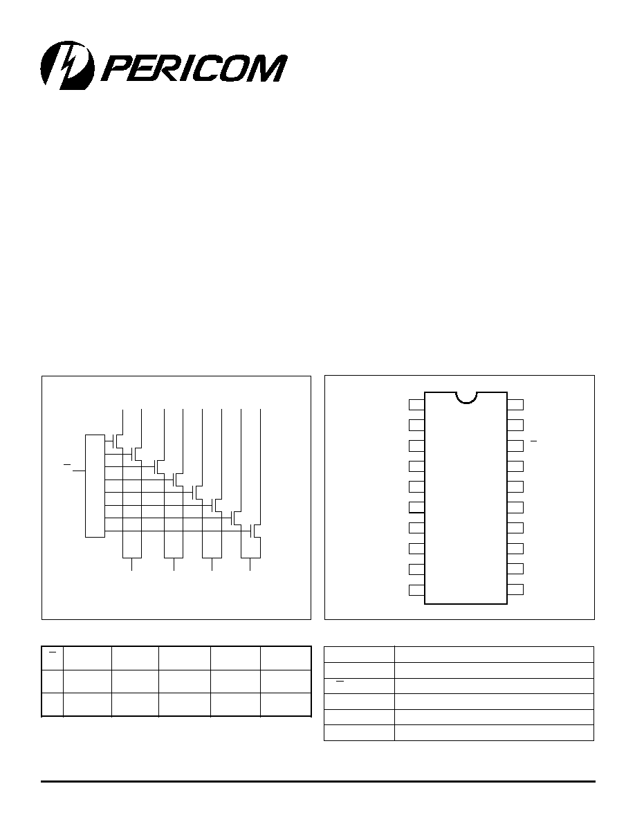
Logic Block Diagram
12345678901234567890123456789012123456789012345678901234567890121234567890123456789012345678901212345678901234567890123456789012123456789012
12345678901234567890123456789012123456789012345678901234567890121234567890123456789012345678901212345678901234567890123456789012123456789012
Truth Table
(1)
Note:
1. H = High Voltage Level
L = Low Voltage Level
Product Pin Description
Pin Name
Description
IAn-IDn
Data Inputs
E
Enable
YA-YD
Data Outputs
GND
Ground
V
CC
Power
PI5L102
CompactPCI
Æ
Hot Swap
Pull-up Switch
Product Features
Supports CompactPCI precharge voltage selection
3.3V/2.7kohms, 5V/1ohm line termination selection
Ultra-low quiescent current: 0.1µA typical
Low ON resistance: 7ohms maximum
Single supply operation up to 6.2V ±5%
Wide bandwidth data rates: >200 Mbps
Compact 20-pin TSSOP package
Mechanical relay replacement
Pin Configuration
E
IA0 IA1 IB0 IB1 IC0 IC1 ID0 ID1
YA
YB
YC
YD
20-Pin
L
Product Description
The PI5L102L CompactPCI Hot Swap Pull-up switch is a Quad 1:2
multiplexer. It is designed to switch the 1V precharge bias voltage
and 10-kohm pull-up resistor connected to the CompactPCI bus
signals during Hot Swap. Each switch can connect eight inputs
(I
An
to I
Dn
) to a given pull-up voltage level.
In addition, the PI5L102 can be used to select 2.7 kohms/3.3V or
1.0 kohm/5V pull-ups for the system card PCI signal lines.
ON resistance is a low 7 ohms maximum and all eight switches are
selected or disabled with a single CMOS/TTL compatible signal. For
general-purpose applications, the PI5L102 can replace mechanical
relays. In network systems, physical layer signals can be switched.
To reduce the insertion loss, the PI5L102 can be powered by a 6.2V
Zener diode.
E
A
Y
B
Y
C
Y
D
Y
n
o
it
c
n
u
F
H
Z
-i
H
Z
-i
H
Z
-i
H
Z
-i
H
el
b
a
si
D
L
1
A
I
,
0
A
I
1
B
I
,
0
B
I
1
C
I
,
0
C
I
1
D
I
,
0
D
I
el
b
a
n
E
CompactPCI is a registered trademark of the PCI Industrial Computer Manufacturers Group

2
PS8491C 02/20/01
12345678901234567890123456789012123456789012345678901234567890121234567890123456789012345678901212345678901234567890123456789012123456789012
PI5L102
CompactPCI Hot Swap Pull-Up Switch
DC Electrical Characteristics
(Over the Operating Range, T
A
= 0∞C to +70∞C, V
CC
= 6.2V, +5%, 2%)
Parameters Description
Test Conditions
(1)
Min.
Typ
(2)
Max.
Units
V
IH
Input HIGH Voltage
Guaranteed Logic HIGH Level
2.4
V
V
IL
Input LOW Voltage
Guaranteed Logic LOW Level
0.5
0.8
V
I
IH
Input HIGH Current
V
CC
= Max., V
IN
= V
CC
±1
µA
I
IL
Input LOW Current
V
CC
= Max., V
IN
= GND
±1
µA
I
OZH
High Impedance Output Current
0
A, B
V
CC
±1
µA
V
IK
Clamp Diode Voltage
V
CC
= Min., I
IN
= 18mA
0.7
1.2
V
I
OS
Short Circuit Current
(3)
A (B) = 0V, B (A) = V
CC
100
mA
V
H
Input Hysteresis at Control Pins
150
mV
R
ON
Switch On Resistance
(4)
V
CC
= Min.,V
IN
= 0.0V I
ON
= 48mA
5
7
V
CC
= Min.,V
IN
= 2.4V I
ON
= 15mA
10
15
Maximum Ratings
(Above which the useful life may be impaired. For user guidelines, not tested.)
Storage Temperature ............................................................65∞C to +150∞C
Ambient Temperature with Power Applied ............................... 0∞C to +70∞C
Supply Voltage to Ground Potential (Inputs & Vcc Only) ......0.5V to +7.0V
Supply Voltage to Ground Potential (Outputs & D/O Only) ...0.5V to +7.0V
DC Input Voltage ....................................................................0.5V to +7.0V
DC Output Current ..............................................................................120mA
Power Dissipation ................................................................................. 0.5W
Note:
Stresses greater than those listed under MAXIMUM
RATINGS may cause permanent damage to the device.
This is a stress rating only and functional operation of
the device at these or any other conditions above
those indicated in the operational sections of this
specification is not implied. Exposure to absolute
maximum rating conditions for extended periods may
affect reliability.
Notes:
1. For Max. or Min. conditions, use appropriate value specified under Electrical Characteristics for the applicable device type.
2. Typical values are at V
CC
= 6.2V, T
A
= 25∞C ambient temperature.
3. Not more than one output should be shorted at one time. Duration of the test should not exceed one second.
4. Measured by voltage drop between I and Y pins at indicated current through the switch. ON resistance is determined by
the lower of the voltages on the two (I,Y) pins.
ohm

PI5L102
CompactPCI Hot Swap Pull-Up Switch
3
PS8491C 02/20/01
12345678901234567890123456789012123456789012345678901234567890121234567890123456789012345678901212345678901234567890123456789012123456789012
Note:
1. This parameter is determined by device characterization, but not production tested.
2. Switch ON Capacitance accounts for capacitance of both switch channels (I
X0
& I
X1
) ON at one time.
3. X = A, B, C, or D; N = 0 or 1
Notes:
1. For Max. or Min. conditions, use appropriate value specified under Electrical Characteristics for the applicable device.
2. Typical values are at V
CC
= 6.2V, T
A
= 25∞C ambient temperature.
3. Per TTL driven input (V
IN
= 3.4V, control inputs only); A and B pins do not contribute to I
CC
.
4. This current applies to the control inputs only and represent the current required to switch internal capacitance at the specified
frequency. The A and B inputs generate no significant AC or DC currents as they transition. This parameter is not tested, but is
guaranteed by design.
Power Supply Characteristics
Parameters Description
Test Conditions
(1)
Min.
Typ
(2)
Max.
Units
I
CC
Quiescent Power
V
CC
= Max.
V
IN
= GND or V
CC
0.1
3.0
µA
Supply Current
I
CC
Supply Current per
V
CC
= Max.
V
IN
= 3.4V
(3)
2.5
mA
Input @ TTL HIGH
I
CCD
Supply Current per
V
CC
= Max.,
0.25
mA/
Input per MHz
(4)
Input Pins Open
MHz
E = GND
Control Input Toggling
50% Duty Cycle
PI5L102
Com.
Parameters
Description
Conditions
(1)
Min.
Typ
Max.
Units
t
PHZ
Bus Disable Time
C
L
= 50pF
0.5
6.0
ns
t
PLZ
E to Y
R
L
= 500ohm
t
PZH
Bus Enable Time
0.5
5.8
ns
t
PZL
E to Y
Notes:
1. See test circuit and waveforms (Figure 2).
Switching Characteristics over Operating Range
s
r
e
t
e
m
a
r
a
P
)
1
(
n
o
it
p
i
r
c
s
e
D
s
n
o
it
i
d
n
o
C
t
s
e
T
.
p
y
T
.
x
a
M
s
ti
n
U
C
N
I
e
c
n
a
ti
c
a
p
a
C
t
u
p
n
I
V
N
I
V
0
=
4
6
F
p
C
F
F
O
)
x
Y
(
Y
X
F
F
O
h
c
ti
w
S
,
e
c
n
a
ti
c
a
p
a
C
6
8
C
)
I(
F
F
O
I
N
X
F
F
O
h
c
ti
w
S
,
e
c
n
a
ti
c
a
p
a
C
6
8
C
)
x
Y
(
N
O
)
2
,
1
(
Y
X
N
O
h
c
ti
w
S
,
e
c
n
a
ti
c
a
p
a
C
4
2
2
3
Capacitance
(T
A
= 25∞C, f = 1 MHz)
XN

4
PS8491C 02/20/01
12345678901234567890123456789012123456789012345678901234567890121234567890123456789012345678901212345678901234567890123456789012123456789012
PI5L102
CompactPCI Hot Swap Pull-Up Switch
Applications
V
CC
Bias Voltage vs R
ON
To keep R
ON
to a minimum, it is recommended that the V
CC
voltage
be increased to a voltage between +6.0V and +6.5V (see Figure 5).
The R
ON
vs V
IN
curve shows the effect of ON-resistance and
input voltage which is exponential. Ideally an input voltage
between 0.2V and 3.6V will keep R
ON
in the flat part of the curve
(
R
ON
or flatness is ~2ohm).
Logic Inputs
The logic control inputs can be driven up to +5.5V regardless of
the supply voltage. For example, given a +5.0V supply, E may be
driven low to 0V and high to 5.5V. Driving E Rail-to-Rail
Æ
minimizes power consumption.
Power-Supply Sequencing
Proper power-supply sequencing is recommended for all CMOS
devices. Always apply V
CC
before applying signals to the input/
output or control pins.
Figure 1. V
IO
Voltage Selection
2.7 k
1 k
PI5AL102
Pullup Required on Each cPCI Line
PI5AL102
10
Enable 3.3V
Pericom
PCI
Bridge
PI7C7100
From cPCI
Connector
Enable 5V
5V
3V
V
IO
V
IO
Figure 2. Hot Swap Precharge Voltage Selection
1.0V
Precharge
10
PI5L102
10k
Resistors
Backplane
HOT SWAP
Connections
E
10

PI5L102
CompactPCI Hot Swap Pull-Up Switch
5
PS8491C 02/20/01
12345678901234567890123456789012123456789012345678901234567890121234567890123456789012345678901212345678901234567890123456789012123456789012
Figure 3. Switching Time
Test Circuits and Waveforms
Pulse
Generator
D.U.T.
V
IN
RT
V
OUT
CL
500
500
open
50pF
V
CC
6V
t
PZL
Control
Input
1.5V
0V
3V
1.5V
3V
0V
1.5V
t
PLZ
V
OL
3V
0V
t
PZH
t
PHZ
0.3V
0.3V
Output
Normally
Low
Output
Normally
High
Switch
Switch
GND
V
OH
Enable
Disable
Enable and Disable Timing
Test Circuits
t
s
e
T
h
c
ti
w
S
W
O
L
d
el
b
a
si
D
W
O
L
d
el
b
a
n
E
d
e
s
o
l
C
Switch Position
DEFINITIONS:
C
L
= Load capacitance: includes jig and probe capacitance.
R
T
= Termination resistance: should be equal to Z
OUT
of
the Pulse Generator
1.
Input Control Enable = Low and Input Control Disable = High
2.
Pulse Generator for All Pulses: Rate - <1.0MHz; ZOUT <50
t
F
, t
R
<2.5 ns.
Figure 5. V
CC
Bias Current
Figure 4. Line Termination
100
120
+V
PI5L102
R
1mA
V
CC
6.2V
ZENER

6
PS8491C 02/20/01
12345678901234567890123456789012123456789012345678901234567890121234567890123456789012345678901212345678901234567890123456789012123456789012
PI5L102
CompactPCI Hot Swap Pull-Up Switch
Figure 6. R
ON
vs Input Voltage over Temperature
(R
ON
at Vcc = 6.1V @ 75∞C)
Figure 7 R
ON
vs Input Voltage
(R
ON
at V
CC
= 6.2V @ 25∞C)
0.000
6.000
0.000
20.00
E+00
2.000/Div.
0.600V/Div.
V
IN
0.000
6.000
0.6000/Div.
V
IN
= 4.5000V, R
ON
= 14.3E+00, V
ON
= 3.9569V
V
ON
R
ON
25∞C
75∞C
75∞C
25∞C
R
ON
V
ON
0.000
6.000
0.000
20.00
E+00
2.000/Div.
0.600V/Div.
V
IN
0.000
6.000
0.6000/Div.
V
IN
= 4.5000V, R
ON
= 10.9E+00, V
ON
= 4.0720V
V
ON
R
ON
R
ON
V
ON

PI5L102
CompactPCI Hot Swap Pull-Up Switch
7
PS8491C 02/20/01
12345678901234567890123456789012123456789012345678901234567890121234567890123456789012345678901212345678901234567890123456789012123456789012
.252
.260
.047
1.20
.002
.006
SEATING
PLANE
.0256
BSC
.018
.030
.004
.008
.238
.269
1
20
.169
.177
X.XX
X.XX
DENOTES CONTROLLING
DIMENSIONS IN MILLIMETERS
0.05
0.15
6.1
6.7
0.45
0.75
0.09
0.20
4.3
4.5
6.4
6.6
0.65
0.19
0.30
.007
.012
Max
20-Pin TSSOP Package Drawing (L)
Pericom Semiconductor Corporation
2380 Bering Drive San Jose, CA 95131 1-800-435-2336 Fax (408) 435-1100 http://www.pericom.com
t
r
a
P
e
g
a
k
c
a
P
-
n
i
P
e
r
u
t
a
r
e
p
m
e
T
L
2
0
1
L
5
I
P
)
L
(
P
O
S
S
T
-
0
2
C
∞
0
7
+
o
t
C
∞
0
Ordering Information