
1
PS8592D 09/22/04
Features
∑
Maximum rated frequency: 133 MHz
∑
Low cycle-to-cycle jitter
∑
Input to output delay, less than 300ps
∑
Internal feedback allows outputs to be synchronized
to the clock input
∑
5V tolerant input*
∑
Spread spectrum clock ready
∑
Operates at 3.3V V
DD
∑
Packaging (Pb-free & Green available):
-8-pin, 150-mil SOIC (W)
-8-pin, 173-mil TSSOP (L)
* CLKIN must reference the same voltage thresholds for the PLL to
deliver zero delay skewing
Description
The PI6C2405A is a PLL based, zero-delay buffer, with the ability
to distribute five outputs of up to 133MHz at 3.3V. All the outputs
are distributed from a single clock input CLKIN and output OUT0
performs zero delay by connecting a feedback to PLL.
An internal feedback on OUT0 is used to synchronize the out-
puts to the input; the relationship between loading of this signal
and the outputs determines the input-output delay. PI6C2405A
is able to track spread spectrum clocking for EMI reduction.
PI6C2405A is characterized for both commercial and industrial
operation.
PI6C2405A-1H is a high-drive version of PI6C2405A-1
Zero-Delay Clock Buffer
PI6C2405A
PLL
CLKIN
OUT
0
OUT
1
OUT
2
OUT
3
OUT
4
PI6C2405A(≠1, ≠1H)
Block Diagram
1
2
3
GND
4
OUT
1
OUT
0
V
DD
OUT
3
8
7
6
5
CLKIN
OUT
2
OUT
4
Pin Configuration
Pin Description
Pin
Signal
Description
1
CLKIN
Input clock reference frequency (weak pull-down)
2, 3, 5, 7
OUT[1-4]
Clock Outputs
4
GND
Ground
6
V
DD
3.3V Supply
8
OUT0
Clockoutput, internal PLL feedback (weak pull-down)
2
PS8592D 09/22/04
PI6C2405A
Zero Delay Clock Buffer
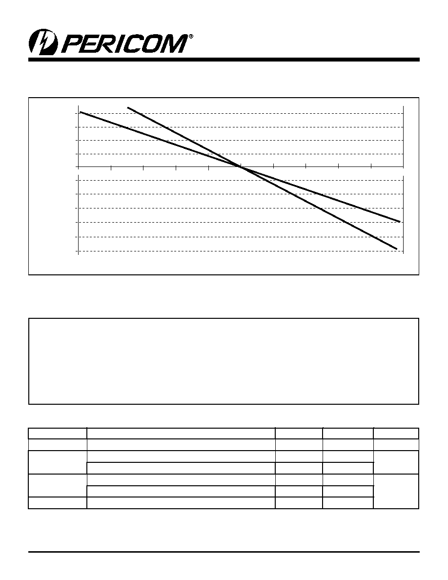
The relationship between loading of the OUT0 signal and other outputs determines the input-output delay. Zero delay is achieved when
all outputs, including feedback, are loaded equally.
Zero Delay and Skew Control
CLKIN Input to OUTx Delay vs. Difference in Loading between OUT0 pin and OUTx pins
Output Load Difference: OUT0 Load - OUTx Load (pF)
CLKIN - Input to OUTx Dela
y (ps)
600
800
400
200
0
-200
-400
-600
-800
-900
-1000
-25
-20
-15
-10
-5
0
5
10
15
20
25
PI6C2405A-1H
PI6C2405A-1
Maximum Ratings
Supply Voltage to Ground Potential............................................................................................................................. ≠0.5V to +7.0V
DC Input Voltage (Except CLKIN)......................................................................................................................≠0.5V to V
DD
+0.5V
DC Input Voltage CLKIN .................................................................................................................................................... ≠0.5 to 7V
Storage Temperature ..................................................................................................................................................≠65∫C to +150∫C
Maximum Soldering Temperature (10 seconds) ......................................................................................................................... 260∫C
Junction Temperature .................................................................................................................................................................. 150∫C
Static Discharge Voltage (per MIL-STD-883, Method 3015).................................................................................................. >2000V
Operating Conditions
(V
CC
= 3.3V ±0.3V)
Parameter
Description
Min.
Max.
Units
V
DD
Supply Voltage
3.0
3.6
V
T
A
Commerical Operating Temperature
0
70
∞C
Industrial Operating Temperature
-40
85
C
L
Load Capacitance, below 100 MHz
30
pF
Load Capacitance, from 100 MHz to 133
15
C
IN
Input Capacitance
7
3
PS8592D 09/22/04
PI6C2405A
Zero Delay Clock Buffer
AC Electrical Characteristics for Industrial Temperature Devices
Parameter
Description
Test Conditions
Min.
Typ.
Max.
Units
F
O
Output Frequency
30pF load
10
100
MHz
15pF load
10
133
t
DC
Duty Cycle
(1)
(-1)
Measured at V
DD
/2, F
OUT
< 66.67MHz, 30pF load
40
50
60
%
Measured at V
DD
/2, F
OUT
< 45MHz 15pF load
45
55
Duty Cycle
(1)
(-1H)
Measured at V
DD
/2, F
OUT
< 100MHz 15pF load
40
60
Measured at V
DD
/2, F
OUT
< 45MHz 30pF load
45
55
t
R
Rise Time
(1)
(-1)
Measured between 0.8V and 2.0V, 30pF load
2.2
ns
Measured between 0.8V and 2.0V, 15pF load
1.5
Rise Time
(1)
(-1H)
Measured between 0.8V and 2.0V, 30pF load
1.5
t
F
Fall Time
(1)
(-1)
Measured between 0.8V and 2.0V, 30pF load
2.2
Measured between 0.8V and 2.0V, 15pF load
1.5
Fall Time
(1)
(-1H)
Measured between 0.8V and 2.0V, 30pF load
1.5
t
sk(o)
Output to Output
skew (-1, -1H)
(1)
All outputs equally loaded
200
ps
t
0
Delay, CLKIN Rising
Edge to OUT0 Rising
Edge
(1)
Measured at V
DD
/2
0
±300
t
SK(D)
Device-to-device
skew
(1)
Measured at V
DD
/2 on OUT0 pins of device
0
600
t
SLEW
Output slew rate
(1)
Measured between 0.8V and 2.0V on -1H device
using Test Circuit #2
1
V/ns
t
JIT
Cycle-to-Cycle Jitter
(-1, -1H)
Measured at 66.67 MHz, loaded 30pF load
200
ps
t
LOCK
PLL Lock time
(1)
Stable power supply, valid clocks presented on
CLKIN pin
1.0
ms
DC Electrical Characteristics for Industrial Temperature Devices
Parameter
Description
Test Conditions
Min.
Max.
Units
V
IL
Input LOW Voltage
0.8
V
V
IH
Input HIGH Voltage
2.0
I
IL
Input LOW Current
V
IN
= 0V
50
µA
I
IH
Input HIGH Current
V
IN
= V
DD
125
V
OL
Output LOW Voltage
I
OL
= -8mA(-1); I
OL
= 12mA(-1H)
0.4
V
V
OH
Output HIGH Voltage
I
OH
= -8mA(-1); I
OH
= -12mA(-1H)
2.4
I
DD
Supply Current
Unloaded outputs 100 MHz, Select inputs at V
DD
or GND
54
mA
Unloaded outputs 66 MHz, CLKIN
39
Notes:
1. See Switching Waveforms on page 5.

4
PS8592D 09/22/04
PI6C2405A
Zero Delay Clock Buffer
AC Electrical Characteristics for Commercial Temperature Devices
Parameter
Description
Test Conditions
Min.
Typ.
Max.
Units
F
O
Output Frequency
30pF load
10
100
MHz
15pF load
10
133
t
DC
Duty Cycle
(1)
(-1)
Measured at V
DD
/2, F
O
< 66 MHz, 30pF load
40
50
60
%
Duty Cycle
(1)
(-1H)
Measured at V
DD
/2, F
O
< 66 MHz, 30pF load
45
50
55
t
R
Rise Time
(1)
@ 30pF
Measured between 0.8V and 2.0V
2.2
ns
Rise Time
(1)
@ 15pF
1.5
Rise Time
(1)
@ 30pF (-1H)
1.5
t
F
Fall Time
(1)
@ 30pF
Measured between 0.8V and 2.0V
2.2
Fall Time
(1)
@ 15pF
1.5
Fall Time
(1)
@ 30pF (-1H)
1.5
t
sk(o)
Output to Output skew (-1,
-1H)
(1)
All outputs equally loaded
200
ps
t
0
Input to output delay,
CLKIN Rising Edge to
OUT0 Rising Edge
(1)
Measured at V
DD
/2
0
±300
t
SK(D)
Device-to-device skew
(1)
Measured at V
DD
/2 on OUT0 pins of device
0
600
t
SLEW
Output slew rate
(1)
Measured between 0.8V and 2.0V on -1H
device using Test Circuit #2
1
V/ns
t
JIT
Cycle-to-Cycle Jitter
(-1, -1H)
Measured at 66.67 MHz, loaded 30pF load
200
ps
t
LOCK
PLL Lock time
(1)
Stable power supply, valid clocks presented
on CLKIN pin
1.0
ms
Notes:
1. See Switching Waveforms on page 5.
DC Electrical Characteristics for Commercial Temperature Devices
Parameter
Description
Test Conditions
Min.
Max.
Units
V
IL
Input LOW Voltage
0.8
V
V
IH
Input HIGH Voltage
2.0
I
IL
Input LOW Current
V
IN
= 0V
50
µA
I
IH
Input HIGH Current
V
IN
= V
DD
125
V
OL
Output LOW Voltage
I
OL
= -8mA(-1); I
OL
= 12mA(-1H)
0.4
V
V
OH
Output HIGH Voltage
I
OH
= -8mA(-1); I
OH
= -12mA(-1H)
2.4
I
DD
Supply Current
Unloaded outputs 100 MHz, Select inputs at V
DD
or GND
54
mA
Unloaded outputs 66.67 MHz, select inputs at V
DD
or GND
39

5
PS8592D 09/22/04
PI6C2405A
Zero Delay Clock Buffer
Switching Waveforms
tlow
thigh
VDD/2
VDD/2
VDD/2
tF
tR
0.8V
2.0V
0.8V
2.0V
OUTPUT
0V
3.3V
VDD/2
VDD/2
VDD/2
VDD/2
VDD/2
VDD/2
tSK(O)
OUTPUT
OUTPUT
t0
INPUT
OUTPUT
tSK(D)
OUTPUT Device 1
OUTPUT Device 2
Duty Cycle Timing
All Outputs Rise/Fall Time
Output-Output Skew
Input-Output Propagation Delay
Device-Device Skew
tDC =
thigh
thigh+tlow
V
DD
CLOAD
V
DD
GND
GND
CLK out
OUTPUTS
0.1µF
0.1µF
V
DD
10pF
V
DD
GND
GND
CLK out
OUTPUTS
0.1µF
0.1µF
1k-ohm
1k-ohm
Test Circuit 2
Test Circuit for tSLEW ,Output slew rate on ≠1H device
Test Circuit 1
Test Circuit for all parameters except t
SLEW

6
PS8592D 09/22/04
PI6C2405A
Zero Delay Clock Buffer
Packaging Mechanical: 8-Pin SOIC (W)
.0040
.0098
SEATING PLANE
.013
.020
.050
BSC
.016
.0075
.0098
1
8
.0099
.0196
0-8∞
.050
.149
.157
X.XX
X.XX
DENOTES DIMENSIONS
IN MILLIMETERS
3.78
3.99
.189
.196
4.80
5.00
1.27
.016
.026
1.35
1.75
.2284
.2440
5.80
6.20
0.406
0.660
0.330
0.508
0.10
0.25
0.40
1.27
0.19
0.25
0.25
0.50
x 45∞
.053
.068
REF
Packaging Mechanical: 8-Pin TSSOP (L)
7
PS8592D 09/22/04
PI6C2405A
Zero Delay Clock Buffer
Pericom Semiconductor Corporation ∑ 1-800-435-2336 ∑ www.pericom.com
Ordering Information for Commercial Operating Ranges
Ordering Code
Package Code
Package Description
PI6C2405A-1W
W
8-pin 150-mil SOIC
PI6C2405A-1WE
W
Pb-free & Green, 8-pin 150-mil SOIC
PI6C2405A-1HW
W
8-pin 150-mil SOIC
PI6C2405A-1HWE
W
Pb-free & Green, 8-pin 150-mil SOIC
PI6C2405A-1L
L
8-pin 173-mil TSSOP
PI6C2405A-1LE
L
Pb-free & Green, 8-pin 173-mil TSSOP
PI6C2405A-1HL
L
8-pin 173-mil TSSOP
PI6C2405A-1HLE
L
Pb-free & Green, 8-pin 173-mil TSSOP
Ordering Information for Industrial Operating Ranges
Ordering Code
Package Code
Package Description
PI6C2405A1WI
W
8-pin 150-mil SOIC
PI6C2405A-1WIE
W
Pb-free & Green, 8-pin 150-mil SOIC
PI6C2405A-1HWI
W
8-pin 150-mil SOIC
PI6C2405A-1HWIE
W
Pb-free & Green, 8-pin 150-mil SOIC
PI6C2405A-1LI
L
8-pin 173-mil TSSOP
PI6C2405A-1LIE
L
Pb-free & Green, 8-pin 173-mil TSSOP
PI6C2405A-1HLI
L
8-pin 173-mil TSSOP
PI6C2405A-1HLIE
L
Pb-free & Green, 8-pin 173-mil TSSOP
Notes:
1. Thermal characteristics can be found on the company web site at www.pericom.com/packaging/
2. X = Tape/Reel