1
PS8589E 09/15/04
Features
∑
Maximum rated frequency: 140 MHz
∑
Low cycle-to-cycle jitter
∑
Input to output delay, less than 150ps
∑
External feedback pin allows outputs to be synchronized
to the clock input
∑
5V tolerant input*
∑
Operates at 3.3V V
DD
∑
Test mode allows bypass of the PLL for system testing
purposes (e.g., IBIS measurements)
∑
Clock frequency multipliers Ωx to 4x dependent on option
∑
Packaging (Pb-free and Green available):
-16-pin, 150-mil SOIC (W)
-16-pin 173-mil TSSOP (L)
Description
The PI6C2408 is a PLL-based, zero-delay buffer, with the ability
to distribute eight outputs of up to 140 MHz at 3.3 V. Two banks of
four outputs exist, and, depending on product option ordered, can
supply either reference frequency, prescaled half frequency, or
multiplied 2x or 4x input clock frequencies. The PI6C2408 family has
a power-sparing feature: when input SEL2 is 0, the component will
3-state one or both banks of outputs depending on the state of input
SEL1. A PLL bypass test mode also exists. This product line is
available in high-drive and industrial environment versions.
An external feedback pin is used to synchronize the outputs to the
input; the relationship between loading of this signal and the other
outputs determines the input-output delay.
The PI6C2408 is characterized for both commercial and industrial
operation.
Block Diagram
Pin Configuration
12345678901234567890123456789012123456789012345678901234567890121234567890123456789012345678901212345678901234567890123456789012123456789012
12345678901234567890123456789012123456789012345678901234567890121234567890123456789012345678901212345678901234567890123456789012123456789012
Zero-Delay Clock Buffer
PI6C2408
* FB_IN and CLKIN must reference the same voltage thresh-
olds for the PLL to deliver zero delay skewing
PLL
Option (-3, -4)
CLKIN
FB_IN
SEL1
SEL2
Decode
Logic
Decode
Logic
OUTA1
OUTA2
OUTA3
OUTA4
OUTB2
OUTB3
OUTB4
OUTB1
PI6C2408 (-1, -1H, -2, -3, -4)
˜2
PLL
CLKIN
FB_IN
SEL2
SEL1
OUTA1
OUTA2
OUTA3
OUTA4
OUTB2
OUTB3
OUTB4
OUTB1
PI6C2408-6
MUX
˜2
˜2
Option (-2, -3)
MUX
MUX
1
2
3
VDD
4
GND
5
OUTA2
6
OUTB2
7
SEL1
8
OUTB1
FB_IN
OUTA3
VDD
OUTB4
OUTB3
SEL2
16
15
14
13
12
11
10
9
CLKIN
OUTA1
GND
OUTA4
16-Pin
W, L
2
PS8589E 09/15/04
12345678901234567890123456789012123456789012345678901234567890121234567890123456789012345678901212345678901234567890123456789012123456789012
12345678901234567890123456789012123456789012345678901234567890121234567890123456789012345678901212345678901234567890123456789012123456789012
PI6C2408
Zero Delay Clock Buffer
2
L
E
S
1
L
E
S
]
4
-
1
[
A
T
U
O
]
4
-
1
[
B
T
U
O
e
c
r
u
o
S
t
u
p
t
u
O
L
L
P
0
0
e
t
a
t
S
-
3
e
t
a
t
S
-
3
L
L
P
F
F
O
0
1
L
L
P
e
t
a
t
S
-
3
L
L
P
N
O
1
0
N
I
K
L
C
N
I
K
L
C
N
I
K
L
C
F
F
O
1
1
L
L
P
L
L
P
L
L
P
N
O
Input Select Decoding for PI6C2408 (-1, -1H,-4)
e
c
i
v
e
D
m
o
r
F
k
c
a
b
d
e
e
F
y
c
n
e
u
q
e
r
F
]
4
-
1
[
A
T
U
O
y
c
n
e
u
q
e
r
F
]
4
-
1
[
B
T
U
O
1
-
8
0
4
2
C
6
I
P
B
T
U
O
r
o
A
T
U
O
N
I
K
L
C
N
I
K
L
C
H
1
-
8
0
4
2
C
6
I
P
B
T
U
O
r
o
A
T
U
O
N
I
K
L
C
N
I
K
L
C
2
-
8
0
4
2
C
6
I
P
A
T
U
O
N
I
K
L
C
2
/
N
I
K
L
C
2
-
8
0
4
2
C
6
I
P
B
T
U
O
N
I
K
L
C
X
2
N
I
K
L
C
3
-
8
0
4
2
C
6
I
P
A
T
U
O
N
I
K
L
C
X
2
N
I
K
L
C
r
o
N
I
K
L
C
)
1
(
3
-
8
0
4
2
C
6
I
P
B
T
U
O
N
I
K
L
C
X
4
N
I
K
L
C
X
2
4
-
8
0
4
2
C
6
I
P
B
T
U
O
r
o
A
T
U
O
N
I
K
L
C
X
2
N
I
K
L
C
X
2
6
-
8
0
4
2
C
6
I
P
A
T
U
O
N
I
K
L
C
2
/
N
I
K
L
C
r
o
N
I
K
L
C
6
-
8
0
4
2
C
6
I
P
B
T
U
O
N
I
K
L
C
X
2
r
o
N
I
K
L
C
N
I
K
L
C
PI6C2408 Configurations
2
L
E
S
1
L
E
S
]
4
-
1
[
A
T
U
O
]
4
-
1
[
B
T
U
O
e
c
r
u
o
S
t
u
p
t
u
O
L
L
P
0
0
e
t
a
t
S
-
3
e
t
a
t
S
-
3
L
L
P
F
F
O
0
1
N
I
K
L
C
2
/
N
I
K
L
C
N
I
K
L
C
F
F
O
1
0
L
L
P
L
L
P
L
L
P
N
O
1
1
L
L
P
2
/
L
L
P
L
L
P
N
O
Input Select
Decoding for PI6C2408-6
Note:
1. Output phase is indeterminant (0∞ or 180∞ from CLKIN)
2
L
E
S
1
L
E
S
]
4
-
1
[
A
T
U
O
]
4
-
1
[
B
T
U
O
e
c
r
u
o
S
t
u
p
t
u
O
L
L
P
0
0
e
t
a
t
S
-
3
e
t
a
t
S
-
3
L
L
P
F
F
O
0
1
L
L
P
e
t
a
t
S
-
3
L
L
P
N
O
1
0
N
I
K
L
C
2
/
N
I
K
L
C
N
I
K
L
C
F
F
O
1
1
L
L
P
L
L
P
L
L
P
N
O
Input Select Decoding for PI6C2408 (-2,-3)

3
12345678901234567890123456789012123456789012345678901234567890121234567890123456789012345678901212345678901234567890123456789012123456789012
12345678901234567890123456789012123456789012345678901234567890121234567890123456789012345678901212345678901234567890123456789012123456789012
PI6C2408
Zero Delay Clock Buffer
PS8589E 09/15/04
The relationship between loading of the FB_IN signal and other outputs determines the input-output delay. Zero delay is achieved when
all outputs, including feedback, are loaded equally.
Zero Delay and Skew Control
CLKIN Input to Output Bank Delay vs. Difference in Loading between FB_IN pin and OUTA/OUTB pins
Maximum Ratings
Supply Voltage to Ground Potential ............................................................................................................................. ≠0.5V to +7.0V
DC Input Voltage (Except CLKIN) ........................................................................................................................ ≠0.5V to V
DD
+0.5V
DC Input Voltage CLKIN ...................................................................................................................................................... ≠0.5 to 7V
Storage Temperature ................................................................................................................................................... ≠65∫C to +150∫C
Maximum Soldering Temperature (10 seconds) ........................................................................................................................... 260∫C
Junction Temperature .................................................................................................................................................................. 150∫C
Static Discharge Voltage (per MIL-STD-883, Method 3015) .................................................................................................... >2000V
n
i
P
l
a
n
g
i
S
n
o
i
t
p
i
r
c
s
e
D
1
N
I
K
L
C
)
n
w
o
d
-l
l
u
p
k
a
e
w
(
y
c
n
e
u
q
e
r
f
e
c
n
e
r
e
f
e
r
k
c
o
l
c
t
u
p
n
I
5
1
,
4
1
,
3
,
2
]
4
-
1
[
A
T
U
O
)
n
w
o
d
-l
l
u
p
k
a
e
w
(
A
k
n
a
B
,t
u
p
t
u
o
k
c
o
l
C
3
1
,
4
V
D
D
y
l
p
p
u
s
V
3
.
3
2
1
,
5
D
N
G
d
n
u
o
r
G
1
1
,
0
1
,
7
,
6
]
4
-
1
[
B
T
U
O
)
n
w
o
d
-l
l
u
p
k
a
e
w
(
B
k
n
a
B
,t
u
p
t
u
o
k
c
o
l
C
8
2
L
E
S
)
p
u
-l
l
u
p
k
a
e
w
(
2
ti
b
,t
u
p
n
i
t
c
e
l
e
S
9
1
L
E
S
)
p
u
-l
l
u
p
k
a
e
w
(
1
ti
b
,t
u
p
n
i
t
c
e
l
e
S
6
1
N
I
_
B
F
t
u
p
n
i
k
c
a
b
d
e
e
f
L
L
P
Pin Description
Output Load Difference: FB_IN Load - OUTA/OUTB Load (pF)
CLKIN - Input to OUT
A/OUTB Dela
y (ps)
600
800
400
200
0
-200
-400
-600
-800
-900
-1000
-25
-20
-15
-10
-5
0
5
10
15
20
25
PI6C2408-1H
PI6C2408-1,2,3,4,6

4
PS8589E 09/15/04
12345678901234567890123456789012123456789012345678901234567890121234567890123456789012345678901212345678901234567890123456789012123456789012
12345678901234567890123456789012123456789012345678901234567890121234567890123456789012345678901212345678901234567890123456789012123456789012
PI6C2408
Zero Delay Clock Buffer
r
e
t
e
m
a
r
a
P
n
o
i
t
p
i
r
c
s
e
D
.
n
i
M
.
x
a
M
s
t
i
n
U
V
D
D
e
g
a
tl
o
V
y
l
p
p
u
S
0
.
3
6
.
3
V
T
A
e
r
u
t
a
r
e
p
m
e
T
g
n
it
a
r
e
p
O
l
a
c
i
r
e
m
m
o
C
0
0
7
C
∫
e
r
u
t
a
r
e
p
m
e
T
g
n
it
a
r
e
p
O
l
a
i
r
t
s
u
d
n
I
0
4
≠
5
8
C
L
z
H
M
0
0
1
w
o
l
e
b
,
e
c
n
a
ti
c
a
p
a
C
d
a
o
L
0
3
F
p
z
H
M
0
4
1
o
t
z
H
M
0
0
1
m
o
r
f
,
e
c
n
a
ti
c
a
p
a
C
d
a
o
L
5
1
C
N
I
e
c
n
a
ti
c
a
p
a
C
t
u
p
n
I
7
Operating Conditions
(V
CC
= 3.3V ±0.3V)
DC Electrical Characteristics for Industrial Temperature Devices
r
e
t
e
m
a
r
a
P
n
o
i
t
p
i
r
c
s
e
D
s
n
o
i
t
i
d
n
o
C
t
s
e
T
.
n
i
M
.
x
a
M
s
t
i
n
U
V
L
I
e
g
a
tl
o
V
W
O
L
t
u
p
n
I
8
.
0
V
V
H
I
e
g
a
tl
o
V
H
G
I
H
t
u
p
n
I
0
.
2
I
L
I
t
n
e
r
r
u
C
W
O
L
t
u
p
n
I
V
N
I
= V
0
0
.
0
5
µ
A
I
H
I
t
n
e
r
r
u
C
H
G
I
H
t
u
p
n
I
V
N
I
= V
D
D
0
.
0
0
1
V
L
O
e
g
a
tl
o
V
W
O
L
t
u
p
t
u
O
I
L
O
I
;
)
6
≠
,
4
≠
,
3
≠
,
2
≠
,
1
≠
(
A
m
8
=
L
O
)
H
1
≠
(
A
m
2
1
=
4
.
0
V
V
H
O
e
g
a
tl
o
V
H
G
I
H
t
u
p
t
u
O
I
H
O
I
;
)
6
≠
,
4
≠
,
3
≠
,
2
≠
,
1
≠
(
A
m
8
≠
=
H
O
)
H
1
≠
(
A
m
2
1
≠
=
4
.
2
I
D
D
)
e
d
o
m
D
P
(
t
n
e
r
r
u
C
y
l
p
p
u
S
n
w
D
r
w
P
)
6
≠
(
0
=
2
L
E
S
;
)
H
1
≠
,
4
≠
,
3
≠
,
2
≠
,
1
≠
(
0
=
1
L
E
S
0
.
5
2
µ
A
I
D
D
t
n
e
r
r
u
C
y
l
p
p
u
S
,
z
H
M
0
0
1
s
t
u
p
t
u
o
d
e
d
a
o
l
n
U
V
t
a
s
t
u
p
n
i
t
c
e
l
e
S
D
D
D
N
G
r
o
0
.
4
5
A
m
)
H
1
≠
(
0
.
0
7
)
H
1
≠
(
t
p
e
c
x
e
,
N
I
K
L
C
,
z
H
M
6
6
s
t
u
p
t
u
o
d
e
d
a
o
l
n
U
0
.
9
3
)
H
1
≠
(
t
p
e
c
x
e
,
N
I
K
L
C
,
z
H
M
3
3
s
t
u
p
t
u
o
d
e
d
a
o
l
n
U
0
.
0
2

5
12345678901234567890123456789012123456789012345678901234567890121234567890123456789012345678901212345678901234567890123456789012123456789012
12345678901234567890123456789012123456789012345678901234567890121234567890123456789012345678901212345678901234567890123456789012123456789012
PI6C2408
Zero Delay Clock Buffer
PS8589E 09/15/04
Notes:
1. See Switching Waveforms on page 7.
s
r
e
t
e
m
a
r
a
P
e
m
a
N
s
n
o
i
t
i
d
n
o
C
t
s
e
T
.
n
i
M
.
p
y
T
.
x
a
M
s
t
i
n
U
F
O
y
c
n
e
u
q
e
r
F
t
u
p
t
u
O
d
a
o
l
F
p
0
3
0
.
0
1
0
0
1
z
H
M
d
a
o
l
F
p
5
1
0
4
1
t
C
D
e
l
c
y
C
y
t
u
D
)
1
(
)
6
≠
,
4
≠
,
3
≠
,
2
≠
,
1
≠
(
V
t
a
d
e
r
u
s
a
e
M
D
D
F
,
2
/
T
U
O
d
a
o
l
F
p
0
3
z
H
M
7
6
.
6
6
<
0
.
0
4
0
5
0
.
0
6
%
V
t
a
d
e
r
u
s
a
e
M
D
D
F
,
2
/
T
U
O
d
a
o
l
F
p
5
1
z
H
M
0
4
1
<
V
t
a
d
e
r
u
s
a
e
M
D
D
F
,
2
/
T
U
O
d
a
o
l
F
p
0
3
z
H
M
5
4
<
0
.
5
4
0
.
5
5
e
l
c
y
C
y
t
u
D
)
1
(
)
H
1
≠
(
V
t
a
d
e
r
u
s
a
e
M
D
D
F
,
2
/
T
U
O
d
a
o
l
F
p
0
3
z
H
M
7
6
.
6
6
<
0
.
5
4
V
t
a
d
e
r
u
s
a
e
M
D
D
F
,
2
/
T
U
O
d
a
o
l
F
p
5
1
z
H
M
0
4
1
<
0
.
0
4
0
.
0
6
V
t
a
d
e
r
u
s
a
e
M
D
D
F
,
2
/
T
U
O
d
a
o
l
F
p
0
3
z
H
M
5
4
<
0
.
5
4
0
.
5
5
t
R
e
m
i
T
e
s
i
R
)
1
(
)
,
4
≠
,
3
≠
,
2
≠
,
1
≠
(
d
a
o
l
F
p
0
3
,
V
0
.
2
d
n
a
V
8
.
0
n
e
e
w
t
e
b
d
e
r
u
s
a
e
M
2
.
2
s
n
d
a
o
l
F
p
5
1
,
V
0
.
2
d
n
a
V
8
.
0
n
e
e
w
t
e
b
d
e
r
u
s
a
e
M
0
5
.
1
e
m
i
T
e
s
i
R
)
1
(
)
H
1
≠
(
d
a
o
l
F
p
0
3
,
V
0
.
2
d
n
a
V
8
.
0
n
e
e
w
t
e
b
d
e
r
u
s
a
e
M
0
5
.
1
t
F
e
m
i
T
ll
a
F
)
1
(
)
,
4
≠
,
3
≠
,
2
≠
,
1
≠
(
d
a
o
l
F
p
0
3
,
V
0
.
2
d
n
a
V
8
.
0
n
e
e
w
t
e
b
d
e
r
u
s
a
e
M
0
5
.
2
d
a
o
l
F
p
5
1
,
V
0
.
2
d
n
a
V
8
.
0
n
e
e
w
t
e
b
d
e
r
u
s
a
e
M
0
5
.
1
e
m
i
T
ll
a
F
)
1
(
)
H
1
≠
(
d
a
o
l
F
p
0
3
,
V
0
.
2
d
n
a
V
8
.
0
n
e
e
w
t
e
b
d
e
r
u
s
a
e
M
5
2
.
1
t
)
O
(
K
S
n
i
h
ti
w
w
e
k
S
t
u
p
t
u
O
o
t
t
u
p
t
u
O
)
6
≠
,
4
≠
,
3
≠
,
2
≠
,
1
≠
(
k
n
a
B
e
m
a
s
)
1
(
d
e
d
a
o
l
y
ll
a
u
q
e
s
t
u
p
t
u
o
ll
A
0
0
2
s
p
w
e
k
S
B
T
U
O
o
t
A
T
U
O
)
1
(
)
4
≠
,
H
1
≠
,
1
≠
(
w
e
k
S
B
T
U
O
o
t
A
T
U
O
)
1
(
)
6
≠
,
3
≠
,
2
≠
(
0
0
4
t
0
e
g
d
E
g
n
i
s
i
R
N
I
K
L
C
,
y
a
l
e
D
e
g
d
E
g
n
i
s
i
R
N
I
_
B
F
o
t
)
1
(
V
t
a
d
e
r
u
s
a
e
M
D
D
2
/
0
0
5
1
±
t
)
D
(
K
S
w
e
k
S
e
c
i
v
e
D
-
o
t
-
e
c
i
v
e
D
)
1
(
V
t
a
d
e
r
u
s
a
e
M
D
D
s
e
c
i
v
e
d
f
o
s
n
i
p
N
I
_
B
F
n
o
2
/
0
0
0
5
t
W
E
L
S
e
t
a
R
w
e
l
S
t
u
p
t
u
O
)
1
(
e
c
i
v
e
d
H
1
≠
n
o
V
0
.
2
&
V
8
.
0
n
e
e
w
t
e
b
d
e
r
u
s
a
e
M
2
#
t
r
C
t
s
e
T
g
n
i
s
u
1
s
n
/
V
t
T
I
J
r
e
tt
i
J
e
l
c
y
C
-
o
t
-
e
l
c
y
C
)
1
(
)
4
≠
,
H
1
≠
,
1
≠
(
d
a
o
l
F
p
0
3
d
e
d
a
o
l
,
z
H
M
7
6
.
6
6
t
a
d
e
r
u
s
a
e
M
0
0
2
s
p
d
a
o
l
F
p
5
1
d
e
d
a
o
l
,
z
H
M
0
4
1
t
a
d
e
r
u
s
a
e
M
0
0
1
r
e
tt
i
J
e
l
c
y
C
-
o
t
-
e
l
c
y
C
)
1
(
)
6
≠
,
3
≠
,
2
≠
(
d
a
o
l
F
p
0
3
d
e
d
a
o
l
,
z
H
M
7
6
.
6
6
t
a
d
e
r
u
s
a
e
M
0
0
4
t
K
C
O
L
e
m
i
T
k
c
o
L
L
L
P
)
1
(
s
k
c
o
l
c
d
il
a
v
,
y
l
p
p
u
s
r
e
w
o
p
e
l
b
a
t
S
s
n
i
p
N
I
_
B
F
d
n
a
N
I
K
L
C
n
o
d
e
t
n
e
s
e
r
p
0
.
1
s
m
AC Elecrical Characteristics for Industrial Temperature Devices

6
PS8589E 09/15/04
12345678901234567890123456789012123456789012345678901234567890121234567890123456789012345678901212345678901234567890123456789012123456789012
12345678901234567890123456789012123456789012345678901234567890121234567890123456789012345678901212345678901234567890123456789012123456789012
PI6C2408
Zero Delay Clock Buffer
Notes:
1. See Switching Waveforms on page 7.
s
r
e
t
e
m
a
r
a
P
e
m
a
N
s
n
o
i
t
i
d
n
o
C
t
s
e
T
.
n
i
M
.
p
y
T
.
x
a
M
s
t
i
n
U
F
O
y
c
n
e
u
q
e
r
F
t
u
p
t
u
O
d
a
o
l
F
p
0
3
0
1
0
0
1
z
H
M
d
a
o
l
F
p
5
1
0
4
1
t
C
D
e
l
c
y
C
y
t
u
D
)
1
(
)
H
1
≠
(
V
t
a
d
e
r
u
s
a
e
M
D
D
t
u
p
t
u
o
e
v
i
r
d
h
g
i
h
r
o
f
,
2
/
5
4
0
5
5
5
%
e
l
c
y
C
y
t
u
D
)
6
≠
,
4
≠
,
3
≠
,
2
≠
,
1
≠
(
V
t
a
d
e
r
u
s
a
e
M
D
D
t
u
p
t
u
o
e
v
i
r
d
l
a
m
r
o
n
r
o
f
,
2
/
0
4
0
5
0
6
t
R
e
m
i
T
e
s
i
R
)
1
(
F
p
0
3
@
V
0
.
2
d
n
a
V
8
.
0
n
e
e
w
t
e
b
d
e
r
u
s
a
e
M
2
.
2
s
n
e
m
i
T
e
s
i
R
)
1
(
F
p
5
1
@
5
.
1
e
m
i
T
e
s
i
R
)
1
(
)
H
1
≠
(
F
p
0
3
@
5
.
1
t
F
e
m
i
T
ll
a
F
)
1
(
F
p
0
3
@
2
.
2
e
m
i
T
ll
a
F
)
1
(
F
p
5
1
@
5
.
1
e
m
i
T
ll
a
F
)
1
(
)
H
1
≠
(
F
p
0
3
@
5
2
.
1
t
)
O
(
K
S
w
e
k
S
t
u
p
t
u
O
o
t
t
u
p
t
u
O
)
1
(
e
m
a
s
n
i
h
ti
w
)
6
≠
,
4
≠
,
3
≠
,
2
≠
,
H
1
≠
,
1
≠
(
k
n
a
b
V
,
d
e
d
a
o
l
y
ll
a
u
q
e
s
t
u
p
t
u
o
ll
A
D
D
2
/
0
0
2
s
p
w
e
k
S
B
T
U
O
o
t
A
T
U
O
)
1
(
)
4
≠
,
H
1
≠
,
1
≠
(
V
,
d
e
d
a
o
l
y
ll
a
u
q
e
s
t
u
p
t
u
o
ll
A
D
D
2
/
0
0
2
w
e
k
S
B
T
U
O
o
t
A
T
U
O
)
1
(
)
6
≠
,
3
≠
,
2
≠
(
V
,
d
e
d
a
o
l
y
ll
a
u
q
e
s
t
u
p
t
u
o
ll
A
D
D
2
/
0
0
4
t
0
N
I
K
L
C
,
y
a
l
e
D
t
u
p
t
u
O
o
t
t
u
p
n
I
e
g
d
E
g
n
i
s
i
R
N
I
_
B
F
o
t
e
g
d
E
g
n
i
s
i
R
)
1
(
V
t
a
d
e
r
u
s
a
e
M
D
D
2
/
0
0
5
1
±
t
)
D
(
K
S
w
e
k
S
e
c
i
v
e
D
o
t
e
c
i
v
e
D
)
1
(
V
t
a
d
e
r
u
s
a
e
M
D
D
s
e
c
i
v
e
d
f
o
s
n
i
p
N
I
_
B
F
n
o
2
/
0
0
0
5
t
W
E
L
S
e
t
a
R
w
e
l
S
t
u
p
t
u
O
)
1
(
H
1
≠
n
o
V
0
.
2
d
n
a
V
8
.
0
n
e
e
w
t
e
b
d
e
r
u
s
a
e
M
2
#
ti
u
c
ri
C
t
s
e
T
g
n
i
s
u
e
c
i
v
e
d
1
s
n
/
V
t
T
I
J
r
e
tt
i
J
e
l
c
y
C
-
o
t
-
e
l
c
y
C
)
1
(
)
4
≠
,
H
1
≠
,
1
≠
(
s
t
u
p
t
u
o
F
p
0
3
d
e
d
a
o
l
,
z
H
M
7
6
.
6
6
t
a
d
e
r
u
s
a
e
M
0
0
2
s
p
s
t
u
p
t
u
o
F
p
5
1
d
e
d
a
o
l
,
z
H
M
0
4
1
t
a
d
e
r
u
s
a
e
M
0
0
1
r
e
tt
i
J
e
l
c
y
C
-
o
t
-
e
l
c
y
C
)
1
(
)
6
≠
,
3
≠
,
2
≠
(
s
t
u
p
t
u
o
F
p
0
3
d
e
d
a
o
l
,
z
H
M
7
.
6
6
t
a
d
e
r
u
s
a
e
M
0
0
4
t
K
C
O
L
e
m
i
T
k
c
o
L
L
L
P
)
1
(
s
k
c
o
l
c
d
il
a
v
,
y
l
p
p
u
s
r
e
w
o
p
e
l
b
a
t
S
s
n
i
p
N
I
_
B
F
d
n
a
N
I
K
L
C
n
o
d
e
t
n
e
s
e
r
p
0
.
1
s
m
AC Electrial Characteristics
for Commercial Temperature Device
DC Electrical Characteristics for Commercial Temperature Devices
r
e
t
e
m
a
r
a
P
n
o
i
t
p
i
r
c
s
e
D
s
n
o
i
t
i
d
n
o
C
t
s
e
T
.
n
i
M
.
x
a
M
s
t
i
n
U
V
L
I
e
g
a
tl
o
V
W
O
L
t
u
p
n
I
8
.
0
V
V
H
I
e
g
a
tl
o
V
H
G
I
H
t
u
p
n
I
0
.
2
I
L
I
t
n
e
r
r
u
C
W
O
L
t
u
p
n
I
V
N
I
= V
0
0
5
µ
A
I
H
I
t
n
e
r
r
u
C
H
G
I
H
t
u
p
n
I
V
N
I
= V
D
D
0
0
1
V
L
O
e
g
a
tl
o
V
W
O
L
t
u
p
t
u
O
I
L
O
I
;
)
6
≠
,
4
≠
,
3
≠
,
2
≠
,
1
≠
(
A
m
8
=
L
O
)
H
1
≠
(
A
m
2
1
=
4
.
0
V
V
H
O
e
g
a
tl
o
V
H
G
I
H
t
u
p
t
u
O
I
H
O
I
;
)
6
≠
,
4
≠
,
3
≠
,
2
≠
,
1
≠
(
A
m
8
≠
=
H
O
)
H
1
≠
(
A
m
2
1
≠
=
4
.
2
I
D
D
)
e
d
o
m
D
P
(
t
n
e
r
r
u
C
y
l
p
p
u
S
n
w
o
D
r
e
w
o
P
)
6
-
(
0
=
2
L
E
S
;
)
H
1
-
,
4
-
,
3
-
,
2
-
,
1
-
(
0
=
1
L
E
S
2
1
µ
A
I
D
D
t
n
e
r
r
u
C
y
l
p
p
u
S
V
t
a
s
t
u
p
n
i
t
c
e
l
e
S
,
z
H
M
7
6
.
6
6
,
s
t
u
p
t
u
o
d
e
d
a
o
l
n
U
D
D
D
N
G
r
o
9
3
A
m
I
D
D
t
n
e
r
r
u
C
y
l
p
p
u
S
V
@
s
t
u
p
n
I
t
c
e
l
e
S
z
H
M
0
0
1
s
t
u
p
t
u
o
d
e
d
a
o
l
n
U
D
D
D
N
G
r
o
4
5
7
12345678901234567890123456789012123456789012345678901234567890121234567890123456789012345678901212345678901234567890123456789012123456789012
12345678901234567890123456789012123456789012345678901234567890121234567890123456789012345678901212345678901234567890123456789012123456789012
PI6C2408
Zero Delay Clock Buffer
PS8589E 09/15/04
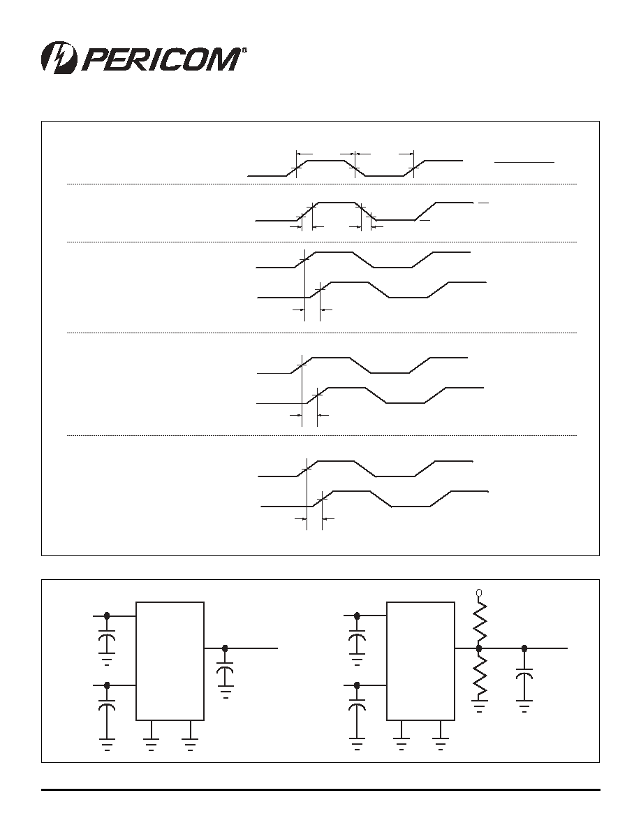
Switching Waveforms
tLOW
tHIGH
VDD/2
VDD/2
VDD/2
tF
tR
0.8V
2.0V
0.8V
2.0V
OUTPUT
0V
3.3V
VDD/2
VDD/2
VDD/2
VDD/2
VDD/2
VDD/2
tSK(O)
OUTPUT
OUTPUT
t0
INPUT
FB_IN
tSK(D)
OUTPUT Device 1
OUTPUT Device 2
Duty Cycle Timing
All Outputs Rise/Fall Time
Output-Output Skew
Input-Output Propagation Delay
Device-Device Skew
tDC =
tHIGH
tLOW
tHIGH +
V
DD
CLOAD
V
DD
GND
GND
CLK out
OUTPUTS
0.1µF
0.1µF
V
DD
10pF
V
DD
GND
GND
CLK out
OUTPUTS
0.1µF
0.1µF
1k-ohm
1k-ohm

8
PS8589E 09/15/04
12345678901234567890123456789012123456789012345678901234567890121234567890123456789012345678901212345678901234567890123456789012123456789012
12345678901234567890123456789012123456789012345678901234567890121234567890123456789012345678901212345678901234567890123456789012123456789012
PI6C2408
Zero Delay Clock Buffer
16-Pin SOIC (W) Package
Note: Controlling dimensions in millimeters. Ref: JEDEC MS - 012 AC
16-Pin TSSOP (L) Package
SEATING PLANE
.050
BSC
1
16
0-8∞
.149
.157
X.XX
X.XX
DENOTES DIMENSIONS
IN MILLIMETERS
3.78
3.99
.386
.393
9.80
10.00
1.27
.053
.068
1.35
1.75
.2284
.2440
5.80
6.20
.0040
.0098
0.10
0.25
.013
.020
.0155
.0260
0.330
0.508
0.393
0.660
.0075
.0098
0.25
0.50
.0099
.0196
x 45∞
0.19
0.25
.016
.050
0.41
1.27
REF
.193
.201
.047
max.
.002
.006
SEATING
PLANE
.0256
BSC
.018
.030
.004
.008
.252
BSC
1
16
.169
.177
X.XX
X.XX
DENOTES CONTROLLING
DIMENSIONS IN MILLIMETERS
0.05
0.15
6.4
0.45
0.75
0.09
0.20
4.3
4.5
1.20
4.9
5.1
0.65
0.19
0.30
.007
.012

9
12345678901234567890123456789012123456789012345678901234567890121234567890123456789012345678901212345678901234567890123456789012123456789012
12345678901234567890123456789012123456789012345678901234567890121234567890123456789012345678901212345678901234567890123456789012123456789012
PI6C2408
Zero Delay Clock Buffer
PS8589E 09/15/04
Ordering Information (Commercial Temperature Device)
Ordering Code
Package
Description
Operating Range
PI6C2408-1W
W
16-pin 150-mil SOIC
Commercial
PI6C2408-1WE
W
Pb-free & Green, 16-pin 150-mil SOIC
Commercial
PI6C2408-1HW
W
16-pin 150-mil SOIC
Commercial
PI6C2408-1HWE
W
Pb-free & Green, 16-pin 150-mil SOIC
Commercial
PI6C2408-2W
W
16-pin 150-mil SOIC
Commercial
PI6C2408-2WE
W
Pb-free & Green, 16-pin 150-mil SOIC
Commercial
PI6C2408-3W
W
16-pin 150-mil SOIC
Commercial
PI6C2408-3WE
W
Pb-free & Green, 16-pin 150-mil SOIC
Commercial
PI6C2408-4W
W
16-pin 150-mil SOIC
Commercial
PI6C2408-4WE
W
Pb-free & Green, 16-pin 150-mil SOIC
Commercial
PI6C2408-6W
W
16-pin 150-mil SOIC
Commercial
PI6C2408-6WE
W
Pb-free & Green, 16-pin 150-mil SOIC
Commercial
PI6C2408-1WE
W
Pb-free & Green 16-pin 150-mil SOIC
Commercial
PI6C2408-1HWE
W
Pb-free & Green 16-pin 150-mil SOIC
Commercial
PI6C2408-1L
L
16-pin 173-mil TSSOP
Commercial
PI6C2408-1LE
L
Pb-free & Green, 16-pin 173-mil TSSOP
Commercial
PI6C2408-1HL
L
16-pin 173-mil TSSOP
Commercial
PI6C2408-1HLE
L
Pb-free & Green, 16-pin 173-mil TSSOP
Commercial
PI6C2408-3L
L
16-pin 173-mil TSSOP
Commercial
PI6C2408-3LE
L
Pb-free & Green, 16-pin 173-mil TSSOP
Commercial
PI6C2408-4L
L
16-pin 173-mil TSSOP
Commercial
PI6c2408-4LE
L
Pb-free & Green, 16-pin 173-mil TSSOP
Commercial
PI6C2408-1LE
L
Pb-free & Green 16-pin 173-mil TSSOP
Commercial
PI6C2408-1HLE
L
Pb-free & Green 16-pin 173-mil TSSOP
Commercial

10
PS8589E 09/15/04
12345678901234567890123456789012123456789012345678901234567890121234567890123456789012345678901212345678901234567890123456789012123456789012
12345678901234567890123456789012123456789012345678901234567890121234567890123456789012345678901212345678901234567890123456789012123456789012
PI6C2408
Zero Delay Clock Buffer
Pericom Semiconductor Corporation ∑ 1-800-435-2336 ∑ www.pericom.com
Ordering Information (Industrial Temperature Device)
Notes:
1. Thermal characteristics can be found on the company web site at www.pericom.com/packaging/
Ordering Code
Package
Description
Operating Range
PI6C2408-1WI
W
16-pin 150-mil SOIC
Industrial
PI6C2408-1WIE
W
Pb-free & Green, 16-pin 150-mil SOIC
Industrial
PI6C2408-1HWI
W
16-pin 150-mil SOIC
Industrial
PI6C2408-1HWIE
W
Pb-free & Green, 16-pin 150-mil SOIC
Industrial
PI6C2408-2WI
W
16-pin 150-mil SOIC
Industrial
PI6C2408-2WIE
W
Pb-free & Green, 16-pin 150-mil SOIC
Industrial
PI6C2408-4WI
W
16-pin 150-mil SOIC
Industrial
PI6C2408-4WIE
W
Pb-free & Green, 16-pin 150-mil SOIC
Industrial
PI6C2408-6WI
W
16-pin 150-mil SOIC
Industrial
PI6C2408-6WIE
W
Pb-free & Green, 16-pin 150-mil SOIC
Industrial
PI6C2408-1LI
L
16-pin 173-mil TSSOP
Industrial
PI6C2408-1LIE
L
Pb-free & Green, 16-pin 173-mil TSSOP
Industrial
PI6C2408-6LI
L
16-pin 173-mil TSSOP
Industrial
PI6C2408-6LIE
L
Pb-free & Green, 16-pin 173-mil TSSOP
Industrial