1
PSXXXX 12/05/01
1
2
3
VDD
4
GND
5
OUTA2
6
OUTB2
7
SEL1
8
OUTB1
OUT0
OUTA3
VDD
OUTB4
OUTB3
SEL2
16
15
14
13
12
11
10
9
CLKIN
OUTA1
GND
OUTA4
Product Features
∑
Maximum rated frequency: 133 MHz
∑
Low cycle-to-cycle jitter
∑
Input to output delay, less than 200ps
∑
Internal feedback allows outputs to be synchronized
to the clock input
∑
5V tolerant input*
∑
Operates at 3.3V V
DD
∑
Space-saving Packages:
150-mil SOIC (W)
173-mil TSSOP (L)
Functional Description
The PI6C240x is a PLL based, zero-delay buffer, with the ability
to distribute five outputs on PI6C2405, nine outputs on PI6C2409 of
up to 133MHz at 3.3V. All the outputs are distributed from a single
clock input CLKIN and output OUT0 performs zero delay by con-
necting a feedback to PLL.
PI6C2409 has two banks of four outputs that can be controlled by
the selection inputs, SEL1 & SEL2. It also has a powersparing feature:
when input SEL1 is 0 and SEL2 is 1, PLL is turned off and all
outputs are referenced from CLKIN. PI6C2405 is an 8-pin version
of PI6C2409 without selection inputs. PI6C240X is available in
high drive and industrial environment versions.
An internal feedback on OUT0 is used to synchronize the outputs
to the input; the relationship between loading of this signal
and the outputs determines the input-output delay.
PI6C240X are characterized for both commercial and industrial
operation
Block Diagram: PI6C2409
Pin Configuration PI6C2409
12345678901234567890123456789012123456789012345678901234567890121234567890123456789012345678901212345678901234567890123456789012123456789012
12345678901234567890123456789012123456789012345678901234567890121234567890123456789012345678901212345678901234567890123456789012123456789012
Zero-Delay Clock Buffer
PI6C2405/PI6C2409
* CLKIN must reference the same voltage thresholds for the
PLL to deliver zero delay skewing
16-Pin
W, L
PLL
CLKIN
SEL1
SEL2
Decode
Logic
OUTA1
OUTA2
OUTA3
OUTA4
OUTB2
OUTB3
OUTB4
OUTB1
PI6C2409 (-1, -1H)
MUX
OUT0
PLL
CLKIN
OUT0
OUT1
OUT2
OUT3
OUT4
PI6C2405(≠1, ≠1H)
Block Diagram: PI6C2405
1
2
3
GND
4
OUT1
OUT0
V
DD
OUT3
8
7
6
5
CLKIN
OUT2
OUT4
Pin Configuration: PI6C2405
8-Pin
W, L

2
PSXXXX 12/05/01
12345678901234567890123456789012123456789012345678901234567890121234567890123456789012345678901212345678901234567890123456789012123456789012
12345678901234567890123456789012123456789012345678901234567890121234567890123456789012345678901212345678901234567890123456789012123456789012
PI6C2405/PI6C2409
Zero Delay Clock Buffer
2
L
E
S
1
L
E
S
]
4
-
1
[
A
T
U
O
]
4
-
1
[
B
T
U
O
e
c
r
u
o
S
t
u
p
t
u
O
)
0
T
U
O
(
L
L
P
0
0
e
t
a
t
S
-
3
e
t
a
t
S
-
3
L
L
P
N
O
0
1
L
L
P
e
t
a
t
S
-
3
L
L
P
N
O
1
0
N
I
K
L
C
N
I
K
L
C
N
I
K
L
C
F
F
O
1
1
L
L
P
L
L
P
L
L
P
N
O
Input Select Decoding for PI6C2409
n
i
P
l
a
n
g
i
S
n
o
it
p
i
r
c
s
e
D
1
N
I
K
L
C
)
n
w
o
d
-l
l
u
p
k
a
e
w
(
y
c
n
e
u
q
e
rf
e
c
n
e
r
e
f
e
r
k
c
o
l
c
t
u
p
n
I
5
1
,
4
1
,
3
,
2
]
4
-
1
[
A
T
U
O
)
n
w
o
d
-l
l
u
p
k
a
e
w
(
A
k
n
a
B
,s
t
u
p
t
u
o
k
c
o
l
C
3
1
,
4
V
D
D
y
l
p
p
u
s
V
3
.
3
2
1
,
5
D
N
G
d
n
u
o
r
G
1
1
,
0
1
,
7
,
6
]
4
-
1
[
B
T
U
O
)
n
w
o
d
-l
l
u
p
k
a
e
w
(
B
k
n
a
B
,s
t
u
p
t
u
o
k
c
o
l
C
8
2
L
E
S
)
p
u
-l
l
u
p
k
a
e
w
(
2
ti
b
,t
u
p
n
i
t
c
el
e
S
9
1
L
E
S
)
p
u
-l
l
u
p
k
a
e
w
(
1
ti
b
,t
u
p
n
i
t
c
el
e
S
6
1
0
T
U
O
)
n
w
o
d
-l
l
u
p
k
a
e
w
(
k
c
a
b
d
e
e
f
L
L
P
l
a
n
r
e
t
n
i
,
t
u
p
t
u
O
k
c
o
l
C
Pin Description for PI6C2409
n
i
P
l
a
n
g
i
S
n
o
it
p
i
r
c
s
e
D
1
N
I
K
L
C
)
n
w
o
d
-l
l
u
p
k
a
e
w
(
y
c
n
e
u
q
e
rf
e
c
n
e
r
e
f
e
r
k
c
o
l
c
t
u
p
n
I
7
,
5
,
3
,
2
]
4
-
1
[
T
U
O
)
n
w
o
d
-l
l
u
p
k
a
e
w
(
,s
t
u
p
t
u
o
k
c
o
l
C
4
D
N
G
y
l
p
p
u
s
V
3
.
3
6
V
D
D
d
n
u
o
r
G
8
0
T
U
O
)
n
w
o
d
-l
l
u
p
k
a
e
w
(
k
c
a
b
d
e
e
f
L
L
P
l
a
n
r
e
t
n
i
,t
u
p
t
u
o
k
c
o
l
C
Pin Description for PI6C2305
3
PSXXXX 12/05/01
12345678901234567890123456789012123456789012345678901234567890121234567890123456789012345678901212345678901234567890123456789012123456789012
12345678901234567890123456789012123456789012345678901234567890121234567890123456789012345678901212345678901234567890123456789012123456789012
PI6C2405/PI6C2409
Zero Delay Clock Buffer
The relationship between loading of the OUT0 signal and other outputs determines the input-output delay. Zero delay is achieved when
all outputs, including feedback, are loaded equally.
Zero Delay and Skew Control
CLKIN Input to OUTx Delay vs. Difference in Loading between OUT0 pin and OUTx pins
Output Load Difference: OUT0 Load - OUTx Load (pF)
CLKIN - Input to OUTx Dela
y (ps)
600
800
400
200
0
-200
-400
-600
-800
-900
-1000
-25
-20
-15
-10
-5
0
5
10
15
20
25
PI6C2405-1H
PI6C2409-1H
PI6C2409-1
PI6C2405-1
Maximum Ratings
Supply Voltage to Ground Potential ............................................................................................................................. 0.5V to +7.0V
DC Input Voltage (Except CLKIN) ........................................................................................................................ 0.5V to V
DD
+0.5V
DC Input Voltage CLKIN ......................................................................................................................................................0.5 to 7V
Storage Temperature ................................................................................................................................................... 65∫C to +150∫C
Maximum Soldering Temperature (10 seconds)........................................................................................................................... 260∫C
Junction Temperature .................................................................................................................................................................. 150∫C
Static Discharge Voltage (per MIL-STD-883, Method 3015) .................................................................................................... >2000V
r
e
t
e
m
a
r
a
P
n
o
it
p
i
r
c
s
e
D
.
n
i
M
.
x
a
M
s
ti
n
U
V
D
D
e
g
a
tl
o
V
y
l
p
p
u
S
0
.
3
6
.
3
V
T
A
e
r
u
t
a
r
e
p
m
e
T
g
n
it
a
r
e
p
O
l
a
ci
r
e
m
m
o
C
0
0
7
C
∫
e
r
u
t
a
r
e
p
m
e
T
g
n
it
a
r
e
p
O
l
ai
rt
s
u
d
n
I
0
4
5
8
C
L
z
H
M
0
0
1
w
o
l
e
b
,
e
c
n
a
ti
c
a
p
a
C
d
a
o
L
æ
0
3
F
p
z
H
M
3
3
1
o
t
z
H
M
0
0
1
m
o
rf
,
e
c
n
a
ti
c
a
p
a
C
d
a
o
L
æ
5
1
C
N
I
e
c
n
a
ti
c
a
p
a
C
t
u
p
n
I
æ
7
Operating Conditions
(V
CC
= 3.3V ±0.3V)

4
PSXXXX 12/05/01
12345678901234567890123456789012123456789012345678901234567890121234567890123456789012345678901212345678901234567890123456789012123456789012
12345678901234567890123456789012123456789012345678901234567890121234567890123456789012345678901212345678901234567890123456789012123456789012
PI6C2405/PI6C2409
Zero Delay Clock Buffer
Notes: 1.See Switching Waveforms on page 6.
s
r
e
t
e
m
a
r
a
P
e
m
a
N
s
n
o
it
i
d
n
o
C
t
s
e
T
.
n
i
M
.
p
y
T
.
x
a
M
s
ti
n
U
F
O
y
c
n
e
u
q
e
r
F
t
u
p
t
u
O
)
H
1
,
1
(
d
a
o
l
F
p
0
3
0
.
0
1
0
0
1
z
H
M
)
H
1
(
,
d
a
o
l
F
p
0
2
3
3
1
)
H
1
,
1
(
,
d
a
o
l
F
p
5
1
t
C
D
el
c
y
C
y
t
u
D
)
1
(
)
1
(
V
t
a
d
e
r
u
s
a
e
M
D
D
F
,
2
/
T
U
O
d
a
o
l
F
p
0
3
z
H
M
7
6
.
6
6
<
0
.
0
4
0
5
0
.
0
6
%
V
t
a
d
e
r
u
s
a
e
M
D
D
F
,
2
/
T
U
O
d
a
o
l
F
p
5
1
z
H
M
5
4
<
0
.
5
4
0
.
5
5
el
c
y
C
y
t
u
D
)
1
(
)
H
1
(
V
t
a
d
e
r
u
s
a
e
M
D
D
F
,
2
/
T
U
O
d
a
o
l
F
p
5
1
z
H
M
3
3
1
<
0
.
0
4
0
.
0
6
V
t
a
d
e
r
u
s
a
e
M
D
D
F
,
V
2
/
T
U
O
d
a
o
l
F
p
0
3
z
H
M
5
4
<
0
.
5
4
0
.
5
5
t
R
e
m
i
T
e
si
R
)
1
(
),
4
,
3
,
2
,
1
(
d
a
o
l
F
p
0
3
,
V
0
.
2
d
n
a
V
8
.
0
n
e
e
w
t
e
b
d
e
r
u
s
a
e
M
2
.
2
s
n
d
a
o
l
F
p
5
1
,
V
0
.
2
d
n
a
V
8
.
0
n
e
e
w
t
e
b
d
e
r
u
s
a
e
M
0
5
.
1
e
m
i
T
e
si
R
)
1
(
)
H
1
(
d
a
o
l
F
p
0
3
,
V
0
.
2
d
n
a
V
8
.
0
n
e
e
w
t
e
b
d
e
r
u
s
a
e
M
0
5
.
1
t
F
e
m
i
T
ll
a
F
)
1
(
)
1
(
d
a
o
l
F
p
0
3
,
V
0
.
2
d
n
a
V
8
.
0
n
e
e
w
t
e
b
d
e
r
u
s
a
e
M
0
5
.
2
d
a
o
l
F
p
5
1
,
V
0
.
2
d
n
a
V
8
.
0
n
e
e
w
t
e
b
d
e
r
u
s
a
e
M
0
5
.
1
e
m
i
T
ll
a
F
)
1
(
)
H
1
(
d
a
o
l
F
p
0
3
,
V
0
.
2
d
n
a
V
8
.
0
n
e
e
w
t
e
b
d
e
r
u
s
a
e
M
5
2
.
1
t
)
O
(
K
S
w
e
k
S
t
u
p
t
u
O
o
t
t
u
p
t
u
O
)
H
1
,
1
(
)
1
(
d
e
d
a
o
l
y
ll
a
u
q
e
st
u
p
t
u
o
ll
A
0
0
2
s
p
t
0
e
g
d
E
g
n
i
si
R
N
I
K
L
C
,y
al
e
D
e
g
d
E
g
n
i
si
R
0
T
U
O
o
t
)
1
(
V
t
a
d
e
r
u
s
a
e
M
D
D
2
/
0
0
0
2
±
t
)
D
(
K
S
w
e
k
S
e
ci
v
e
D
-
o
t
-
e
ci
v
e
D
)
1
(
V
t
a
d
e
r
u
s
a
e
M
D
D
s
e
ci
v
e
d
f
o
s
n
i
p
0
T
U
O
n
o
2
/
0
0
0
6
t
W
E
L
S
e
t
a
R
w
el
S
t
u
p
t
u
O
)
1
(
e
ci
v
e
d
H
1
n
o
V
0
.
2
&
V
8
.
0
n
e
e
w
t
e
b
d
e
r
u
s
a
e
M
2
#
tr
C
t
s
e
T
g
n
i
s
u
1
s
n
/
V
t
T
I
J
r
e
tt
i
J
el
c
y
C
-
o
t
-
el
c
y
C
)
1
(
)
H
1
,
1
(
d
a
o
l
F
p
0
3
d
e
d
a
o
l
,z
H
M
7
6
.
6
6
t
a
d
e
r
u
s
a
e
M
0
0
2
s
p
d
a
o
l
F
p
5
1
d
e
d
a
o
l
,z
H
M
3
3
1
t
a
d
e
r
u
s
a
e
M
0
0
1
t
K
C
O
L
e
m
i
T
k
c
o
L
L
L
P
)
1
(
s
k
c
o
l
c
d
il
a
v
,y
l
p
p
u
s
r
e
w
o
p
el
b
a
t
S
n
i
p
N
I
K
L
C
n
o
d
e
t
n
e
s
e
r
p
0
.
1
s
m
AC Electrical Characteristics for Industrial Temperature Devices
DC Electrical Characteristics for Industrial Temperature Devices
r
e
t
e
m
a
r
a
P
n
o
it
p
i
r
c
s
e
D
s
n
o
it
i
d
n
o
C
t
s
e
T
.
n
i
M
.
x
a
M
s
ti
n
U
V
L
I
e
g
a
tl
o
V
W
O
L
t
u
p
n
I
8
.
0
V
V
H
I
e
g
a
tl
o
V
H
G
I
H
t
u
p
n
I
0
.
2
I
L
I
t
n
e
rr
u
C
W
O
L
t
u
p
n
I
V
N
I
= V
0
0
.
0
5
mA
I
H
I
t
n
e
rr
u
C
H
G
I
H
t
u
p
n
I
V
N
I
= V
D
D
0
.
0
0
1
V
L
O
e
g
a
tl
o
V
W
O
L
t
u
p
t
u
O
I
L
O
I
;)
1
(
A
m
8
=
L
O
)
H
1
(
A
m
2
1
=
4
.
0
V
V
H
O
e
g
a
tl
o
V
H
G
I
H
t
u
p
t
u
O
I
H
O
I
;)
1
(
A
m
8
=
H
O
)
H
1
(
A
m
2
1
=
4
.
2
I
D
D
(
C
6
I
P
)
9
0
3
2
F
F
O
L
L
P
,s
s
a
p
y
B
1
=
2
L
E
S
,
0
=
1
L
E
S
0
.
5
2
mA
I
D
D
t
n
e
rr
u
C
y
l
p
p
u
S
V
t
a
st
u
p
n
i
t
c
el
e
S
,z
H
M
0
0
1
st
u
p
t
u
o
d
e
d
a
o
l
n
U
D
D
D
N
G
r
o
0
.
4
5
A
m
N
I
K
L
C
,z
H
M
6
6
st
u
p
t
u
o
d
e
d
a
o
l
n
U
0
.
9
3

5
PSXXXX 12/05/01
12345678901234567890123456789012123456789012345678901234567890121234567890123456789012345678901212345678901234567890123456789012123456789012
12345678901234567890123456789012123456789012345678901234567890121234567890123456789012345678901212345678901234567890123456789012123456789012
PI6C2405/PI6C2409
Zero Delay Clock Buffer
Notes:
1. See Switching Waveforms on page 6
s
r
e
t
e
m
a
r
a
P
e
m
a
N
s
n
o
it
i
d
n
o
C
t
s
e
T
.
n
i
M
.
p
y
T
.
x
a
M
s
ti
n
U
F
O
y
c
n
e
u
q
e
r
F
t
u
p
t
u
O
)
H
1
,
1
(
d
a
o
l
F
p
0
3
0
1
0
0
1
z
H
M
)
H
1
(
,
d
a
o
l
F
p
0
2
3
3
1
)
H
1
,
1
(
,
d
a
o
l
F
p
5
1
t
C
D
el
c
y
C
y
t
u
D
)
1
(
)
H
1
(
V
t
a
d
e
r
u
s
a
e
M
D
D
F
,
2
/
O
F
p
0
3
,z
H
M
6
6
<
5
4
0
5
5
5
%
el
c
y
C
y
t
u
D
)
1
(
V
t
a
d
e
r
u
s
a
e
M
D
D
F
,
2
/
O
F
p
0
3
,z
H
M
6
6
<
0
4
0
5
0
6
t
R
e
m
i
T
e
si
R
)
1
(
F
p
0
3
@
V
0
.
2
d
n
a
V
8
.
0
n
e
e
w
t
e
b
d
e
r
u
s
a
e
M
2
.
2
s
n
e
m
i
T
e
si
R
)
1
(
F
p
5
1
@
5
.
1
e
m
i
T
e
si
R
)
1
(
)
H
1
(
F
p
0
3
@
5
.
1
t
F
e
m
i
T
ll
a
F
)
1
(
F
p
0
3
@
2
.
2
e
m
i
T
ll
a
F
)
1
(
F
p
5
1
@
5
.
1
e
m
i
T
ll
a
F
)
1
(
)
H
1
(
F
p
0
3
@
5
2
.
1
t
)
O
(
K
S
w
e
k
S
t
u
p
t
u
O
o
t
t
u
p
t
u
O
)
1
(
)
H
1
,
1
(
V
,
d
e
d
a
o
l
y
ll
a
u
q
e
st
u
p
t
u
o
ll
A
D
D
2
/
0
0
2
s
p
t
0
N
I
K
L
C
,y
al
e
D
t
u
p
t
u
O
o
t
t
u
p
n
I
e
g
d
E
g
n
i
si
R
0
T
U
O
o
t
e
g
d
E
g
n
i
si
R
)
1
(
V
t
a
d
e
r
u
s
a
e
M
D
D
2
/
0
0
0
2
±
t
)
D
(
K
S
w
e
k
S
e
ci
v
e
D
o
t
e
ci
v
e
D
)
1
(
V
t
a
d
e
r
u
s
a
e
M
D
D
s
e
ci
v
e
d
f
o
s
n
i
p
0
T
U
O
n
o
2
/
0
0
0
6
t
W
E
L
S
e
t
a
R
w
el
S
t
u
p
t
u
O
)
1
(
H
1
n
o
V
0
.
2
d
n
a
V
8
.
0
n
e
e
w
t
e
b
d
e
r
u
s
a
e
M
2
#
ti
u
c
ri
C
t
s
e
T
g
n
i
s
u
e
ci
v
e
d
1
s
n
/
V
t
T
I
J
r
e
tt
i
J
el
c
y
C
-
o
t
-
el
c
y
C
)
1
(
)
H
1
,
1
(
st
u
p
t
u
o
F
p
0
3
d
e
d
a
o
l
,z
H
M
7
6
.
6
6
t
a
d
e
r
u
s
a
e
M
0
0
2
s
p
st
u
p
t
u
o
F
p
5
1
d
e
d
a
o
l
,z
H
M
3
3
1
t
a
d
e
r
u
s
a
e
M
0
0
1
t
K
C
O
L
e
m
i
T
k
c
o
L
L
L
P
)
1
(
s
k
c
o
l
c
d
il
a
v
,y
l
p
p
u
s
r
e
w
o
p
el
b
a
t
S
s
n
i
p
N
I
K
L
C
n
o
d
e
t
n
e
s
e
r
p
0
.
1
s
m
AC Electrical Characteristics
for Commercial Temperature Device
DC Electrical Characteristics for Commercial Temperature Devices
r
e
t
e
m
a
r
a
P
n
o
it
p
ir
c
s
e
D
s
n
o
it
i
d
n
o
C
t
s
e
T
.
n
i
M
.
x
a
M
s
ti
n
U
V
L
I
e
g
a
tl
o
V
W
O
L
t
u
p
n
I
æ
æ
8
.
0
V
V
H
I
e
g
a
tl
o
V
H
G
I
H
t
u
p
n
I
æ
0
.
2
æ
I
L
I
t
n
e
rr
u
C
W
O
L
t
u
p
n
I
V
N
I
= V
0
æ
0
5
mA
I
H
I
t
n
e
rr
u
C
H
G
I
H
t
u
p
n
I
V
N
I
= V
D
D
æ
0
0
1
V
L
O
e
g
a
tl
o
V
W
O
L
t
u
p
t
u
O
I
L
O
I
;)
1
(
A
m
8
=
L
O
)
H
1
(
A
m
2
1
=
æ
4
.
0
V
V
H
O
e
g
a
tl
o
V
H
G
I
H
t
u
p
t
u
O
I
H
O
I
;)
1
(
A
m
8
=
H
O
)
H
1
(
A
m
2
1
=
4
.
2
æ
I
D
D
)
9
0
3
2
C
6
I
P
(
ff
o
L
L
P
,s
s
a
p
y
B
1
=
2
L
E
S
0
=
1
L
E
S
æ
5
2
mA
I
D
D
t
n
e
rr
u
C
yl
p
p
u
S
V
t
a
st
u
p
n
i
t
c
el
e
S
,z
H
M
7
6
.
6
6
,s
t
u
p
t
u
o
d
e
d
a
o
l
n
U
D
D
D
N
G
r
o
æ
9
3
A
m
I
D
D
t
n
e
rr
u
C
yl
p
p
u
S
V
@
st
u
p
n
I
t
c
el
e
S
z
H
M
0
0
1
st
u
p
t
u
o
d
e
d
a
o
l
n
U
D
D
D
N
G
r
o
æ
4
5
6
PSXXXX 12/05/01
12345678901234567890123456789012123456789012345678901234567890121234567890123456789012345678901212345678901234567890123456789012123456789012
12345678901234567890123456789012123456789012345678901234567890121234567890123456789012345678901212345678901234567890123456789012123456789012
PI6C2405/PI6C2409
Zero Delay Clock Buffer
Switching Waveforms
tlow
thigh
VDD/2
VDD/2
VDD/2
tF
tR
0.8V
2.0V
0.8V
2.0V
OUTPUT
0V
3.3V
VDD/2
VDD/2
VDD/2
VDD/2
VDD/2
VDD/2
tSK(O)
OUTPUT
OUTPUT
t0
INPUT
OUTPUT
tSK(D)
OUTPUT Device 1
OUTPUT Device 2
Duty Cycle Timing
All Outputs Rise/Fall Time
Output-Output Skew
Input-Output Propagation Delay
Device-Device Skew
tDC =
thigh
thigh+tlow
VDD
CLOAD
VDD
GND
GND
CLK out
OUTPUTS
Test Circuit 1
Test Circuit 2
0.1µF
0.1µF
Test Circuit for all parameters except t
SLEW
VDD
10pF
VDD
GND
GND
CLK out
OUTPUTS
0.1µF
0.1µF
Test Circuit for t
SLEW
,Output slew rate on ≠1H device
1k
9
1k
9
7
PSXXXX 12/05/01
12345678901234567890123456789012123456789012345678901234567890121234567890123456789012345678901212345678901234567890123456789012123456789012
12345678901234567890123456789012123456789012345678901234567890121234567890123456789012345678901212345678901234567890123456789012123456789012
PI6C2405/PI6C2409
Zero Delay Clock Buffer
8-Pin SOIC (W) Package
SEATING PLANE
.050
BSC
1
16
0-8∞
.149
.157
X.XX
X.XX
DENOTES DIMENSIONS
IN MILLIMETERS
3.78
3.99
.386
.393
9.80
10.00
1.27
.053
.068
1.35
1.75
.2284
.2440
5.80
6.20
.0040
.0098
0.10
0.25
.013
.020
.0155
.0260
0.330
0.508
0.393
0.660
.0075
.0098
0.25
0.50
.0099
.0196
x 45∞
0.19
0.25
.016
.050
0.41
1.27
REF
.0040
.0098
SEATING PLANE
.013
.020
.050
BSC
.016
.0075
.0098
1
8
.0099
.0196
0-8∞
.050
.149
.157
X.XX
X.XX
DENOTES DIMENSIONS
IN MILLIMETERS
3.78
3.99
.189
.196
4.80
5.00
1.27
.016
.026
1.35
1.75
.2284
.2440
5.80
6.20
0.406
0.660
0.330
0.508
0.10
0.25
0.40
1.27
0.19
0.25
0.25
0.50
x 45∞
.053
.068
REF
16-Pin SOIC (W) Package
8
PSXXXX 12/05/01
12345678901234567890123456789012123456789012345678901234567890121234567890123456789012345678901212345678901234567890123456789012123456789012
12345678901234567890123456789012123456789012345678901234567890121234567890123456789012345678901212345678901234567890123456789012123456789012
PI6C2405/PI6C2409
Zero Delay Clock Buffer
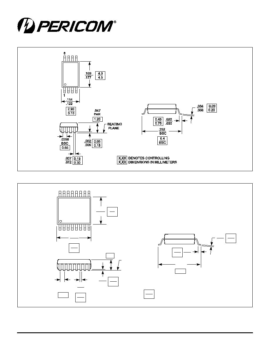
Note: Controlling dimensions in millimeters. Ref: JEDEC MS - 012 AC
16-Pin TSSOP (L) Package
.193
.201
.047
max.
.002
.006
SEATING
PLANE
.0256
BSC
.018
.030
.004
.008
.252
BSC
1
16
.169
.177
X.XX
X.XX
DENOTES CONTROLLING
DIMENSIONS IN MILLIMETERS
0.05
0.15
6.4
0.45
0.75
0.09
0.20
4.3
4.5
1.20
4.9
5.1
0.65
0.19
0.30
.007
.012
8-Pin TSSOP (L) Package

9
PSXXXX 12/05/01
12345678901234567890123456789012123456789012345678901234567890121234567890123456789012345678901212345678901234567890123456789012123456789012
12345678901234567890123456789012123456789012345678901234567890121234567890123456789012345678901212345678901234567890123456789012123456789012
PI6C2405/PI6C2409
Zero Delay Clock Buffer
Pericom Semiconductor Corporation
2380 Bering Drive San Jose, CA 95131 1-800-435-2336 Fax (408) 435-1100 http://www.pericom.com
e
d
o
C
g
n
i
r
e
d
r
O
e
m
a
N
e
g
a
k
c
a
P
e
p
y
T
e
g
a
k
c
a
P
e
g
n
a
R
g
n
it
a
r
e
p
O
W
1
-
9
0
4
2
C
6
I
P
6
1
W
C
I
O
S
li
m
-
0
5
1
n
i
p
-
6
1
l
ai
c
r
e
m
m
o
C
W
H
1
-
9
0
4
2
C
6
I
P
L
1
-
9
0
4
2
C
6
I
P
6
1
L
P
O
S
S
T
n
i
p
-
6
1
L
H
1
-
9
0
4
2
C
6
I
P
I
W
1
-
9
0
4
2
C
6
I
P
6
1
W
C
I
O
S
li
m
-
0
5
1
n
i
p
-
6
1
l
ai
rt
s
u
d
n
I
I
W
H
1
-
9
0
4
2
C
6
I
P
I
L
1
-
9
0
4
2
C
6
I
P
6
1
L
P
O
S
S
T
n
i
p
-
6
1
I
L
H
1
-
9
0
4
2
C
6
I
P
Ordering Information PI6C2409
e
d
o
C
g
n
i
r
e
d
r
O
e
m
a
N
e
g
a
k
c
a
P
e
p
y
T
e
g
a
k
c
a
P
e
g
n
a
R
g
n
it
a
r
e
p
O
W
1
-
5
0
4
2
C
6
I
P
8
W
C
I
O
S
li
m
-
0
5
1
n
i
p
-
8
l
ai
c
r
e
m
m
o
C
W
H
1
-
5
0
4
2
C
6
I
P
L
1
-
5
0
4
2
C
6
I
P
8
L
P
O
S
S
T
n
i
p
-
8
L
H
1
-
5
0
4
2
C
6
I
P
I
W
1
-
5
0
4
2
C
6
I
P
8
W
C
I
O
S
li
m
-
0
5
1
n
i
p
-
8
l
ai
rt
s
u
d
n
I
I
W
H
1
-
5
0
4
2
C
6
I
P
I
L
1
-
5
0
4
2
C
6
I
P
8
1
L
P
O
S
S
T
n
i
p
-
8
I
L
H
1
-
5
0
4
2
C
6
I
P
Ordering Information PI6C2305