PI6C3Q991A
1
PS8628A 02/06/03
Features
· PI6C3Q99X family provides following products:
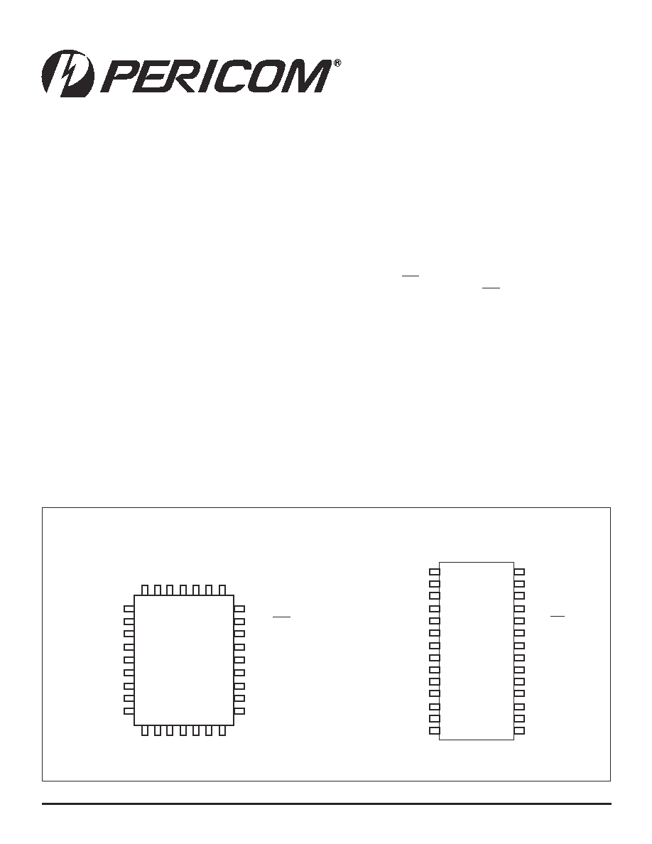
PI6C3Q991A: 32-pin PLCC version
PI6C3Q993A: 28-pin QSOP version
· Inputs are 5V Tolerant
· 4 pairs of programmable skew outputs
· Low skew: 200ps same pair; 250ps all outputs
· Selectable positive or negative edge synchronization:
Excellent for DSP applications
· Synchronous output enable
· Input frequency: 3.75 MHz to 110 MHz
· Output frequency: 15 MHz to 110 MHz
· 2x, 4x, 1/2, and 1/4 outputs
· 3 skew grades:
PI6C3Q99x: t
SKEW0
<750ps
PI6C3Q99x-5: t
SKEW0
<500ps
PI6C3Q99x-2: t
SKEW0
<250ps
· 3-level inputs for skew and PLL range control
· PLL bypass for DC testing
· External feedback, internal loop filter
· 12mA balanced drive outputs
· Low Jitter: < 200ps peak-to-peak
· Industrial temperature range
· Pin-to-pin compatible with IDT QS5V991A and QS5V993A
· Available in 32-pin PLCC and 28-pin QSOP
Description
The PI6C3Q99X family, a high-fanout 3.3V PLL-based clock driver,
is intended for high-performance computing and data-communica-
tion applications. A key feature of the programmable skew is the
ability of outputs to lead or lag the REF input signal. The PI6C3Q991A
has 8 programmable skew outputs in 4 banks of 2, while the
PI6C3Q993A has 6 programmable skew outputs and 2 zero skew
outputs. Skew is controlled by 3-level input signals that may be
hard-wired to appropriate HIGH-MID-LOW levels.
When the GND/sOE pin is held LOW, all the outputs are synchro-
nously enabled. However, if GND/sOE is held HIGH, all outputs
except 3Q0 and 3Q1 are synchronously disabled. Furthermore,
when the V
CCQ
/PE is held HIGH, all outputs are synchronized with
the positive edge of the REF clock input. When V
CCQ
/PE is held
LOW, all outputs are synchronized with the negative edge of REF.
Both devices have LVTTL outputs with 12mA balanced drive
outputs.
Pin Configurations
12345678901234567890123456789012123456789012345678901234567890121234567890123456789012345678901212345678901234567890123456789012123456789012
12345678901234567890123456789012123456789012345678901234567890121234567890123456789012345678901212345678901234567890123456789012123456789012
PI6C3Q991A, PI6C3Q993A
3.3V Programmable Skew PLL Clock Driver
SuperClock
REF
VCCQ
FS
3F0
3F1
VCCQ/PE
VCCN
4Q1
4Q0
GND
3Q1
3Q0
VCCN
FB
GND
TEST
2F1
2F0
GND/sOE
1F1
1F0
VCCN
1Q0
1Q1
GND
GND
2Q0
2Q1
28
27
26
25
24
23
22
21
20
19
18
17
16
15
1
2
3
4
5
6
7
8
9
10
11
12
13
14
2F0
GND/sOE
1F1
1F0
VCCN
1Q0
1Q1
GND
GND
3F1
4F0
4F1
VCCQ/PE
VCCN
4Q1
4Q0
GND
GND
5
6
7
8
9
10
11
12
13
29
28
27
26
25
24
23
22
21
3Q1
3Q0
V
CCN
FB
V
CCN
2Q1
2Q0
3F0
FS
V
CCQ
REF
GND
TEST
2F1
4 3 2 1 32 31 30
14 15 16 17 18 19 20
PI6C3Q993A
PI6C3Q991A
28-Pin
Q
32-Pin
J
12345678901234567890123456789012123456789012345678901234567890121234567890123456789012345678901212345678901234567890123456789012123456789012
12345678901234567890123456789012123456789012345678901234567890121234567890123456789012345678901212345678901234567890123456789012123456789012
PI6C3Q991A, PI6C3Q993A
3.3V Programmable Skew PLL Clock Driver SuperClock
2
PS8628A 02/06/03
Table 1. Pin Descriptions
e
m
a
N
n
i
P
e
p
y
T
n
o
i
t
p
i
r
c
s
e
D
l
a
n
o
i
t
c
n
u
F
F
E
R
N
I
t
u
p
n
i
k
c
o
l
C
e
c
n
e
r
e
f
e
R
B
F
N
I
t
u
p
n
I
k
c
a
b
d
e
e
F
T
S
E
T
)
1
(
N
I
w
e
k
S
.
s
t
u
p
t
u
o
ll
a
o
t
s
e
o
g
F
E
R
.
)
1
e
t
o
N
f
o
s
n
o
it
i
d
n
o
c
r
o
f
t
p
e
c
x
e
(
L
L
P
s
e
l
b
a
s
i
d
,
H
G
I
H
r
o
D
I
M
n
e
h
W
.
n
o
it
a
r
e
p
o
l
a
m
r
o
n
r
o
f
W
O
L
t
e
S
.t
c
e
f
f
e
n
i
n
i
a
m
e
r
)
3
e
l
b
a
t
e
e
s
(
s
n
o
it
c
e
l
e
s
E
O
s
/
D
N
G
)
1
(
N
I
-
e
t
a
t
s
W
O
L
a
n
i
)
1
Q
3
d
n
a
0
Q
3
t
p
e
c
x
e
(
s
t
u
p
t
u
o
k
c
o
l
c
s
p
o
t
s
ti
,
H
G
I
H
n
e
h
W
.
e
l
b
a
n
E
t
u
p
t
u
O
s
u
o
n
o
r
h
c
n
y
S
l
e
v
e
l
D
I
M
t
a
d
l
e
h
s
i
T
S
E
T
n
e
h
W
.
k
c
o
l
e
s
a
h
p
n
i
a
t
n
i
a
m
o
t
l
a
n
g
i
s
k
c
a
b
d
e
e
f
e
h
t
s
a
d
e
s
u
e
b
y
a
m
1
Q
3
r
o
0
Q
3
=
]
0
:
1
[
F
n
n
e
h
w
s
k
n
a
b
l
a
u
d
i
v
i
d
n
i
r
o
f
s
l
o
r
t
n
o
c
e
l
b
a
s
i
d
t
u
p
t
u
o
s
a
t
c
a
s
n
i
p
]
0
:
1
[
F
n
e
h
t
,
H
G
I
H
s
i
E
O
s
/
D
N
G
d
n
a
.
n
o
it
a
r
e
p
o
l
a
m
r
o
n
r
o
f
W
O
L
E
O
s
/
D
N
G
t
e
S
.
L
L
V
Q
C
C
E
P
/
N
I
e
h
t
h
ti
w
d
e
z
i
n
o
r
h
c
n
y
s
e
r
a
s
t
u
p
t
u
o
e
h
t
H
G
I
H
/
W
O
L
n
e
h
W
.l
o
r
t
n
o
c
e
g
d
e
e
v
it
a
g
e
n
r
o
e
v
it
i
s
o
p
e
l
b
a
t
c
e
l
e
S
.
k
c
o
l
c
e
c
n
e
r
e
f
e
r
e
h
t
f
o
e
g
d
e
e
v
it
i
s
o
p
/
e
v
it
a
g
e
n
]
0
:
1
[
F
n
N
I
.
e
g
n
a
r
y
c
n
e
u
q
e
r
f
r
o
s
p
a
t
w
e
k
s
9
f
o
1
g
n
it
c
e
l
e
s
r
o
f
s
t
u
p
n
i
l
e
v
e
l
-
3
S
F
N
I
2
e
l
b
a
t
e
e
S
.
e
g
n
a
r
y
c
n
e
u
q
e
r
f
d
e
t
a
p
i
c
it
n
a
n
o
d
e
s
a
b
ti
u
c
ri
c
r
o
t
a
ll
i
c
s
o
e
t
a
i
r
p
o
r
p
p
a
s
t
c
e
l
e
S
]
0
:
1
[
Q
n
T
U
O
w
e
k
s
o
r
e
z
d
e
x
if
e
r
a
0
:
1
Q
4
A
3
9
9
Q
3
C
6
I
P
e
h
t
n
O
.
w
e
k
s
e
l
b
a
m
m
a
r
g
o
r
p
h
ti
w
,
s
t
u
p
t
u
o
2
f
o
s
k
n
a
b
t
u
p
t
u
o
4
.
s
t
u
p
t
u
o
V
N
C
C
R
W
P
s
r
e
f
f
u
b
t
u
p
t
u
o
r
o
f
y
l
p
p
u
s
r
e
w
o
P
V
Q
C
C
R
W
P
y
r
ti
u
c
ri
c
l
a
n
r
e
t
n
i
r
e
h
t
o
d
n
a
p
o
o
l
d
e
k
c
o
l
e
s
a
h
p
r
o
f
y
l
p
p
u
s
r
e
w
o
P
D
N
G
R
W
P
d
n
u
o
r
G
Note:
1. When TEST = MID and GND/sOE = HIGH, PLL remains active with nF[1:0] =LL functioning as an output disable control for
individual output banks. Skew selections (see Table 3) remain in effect unless nF[1:0] = LL.
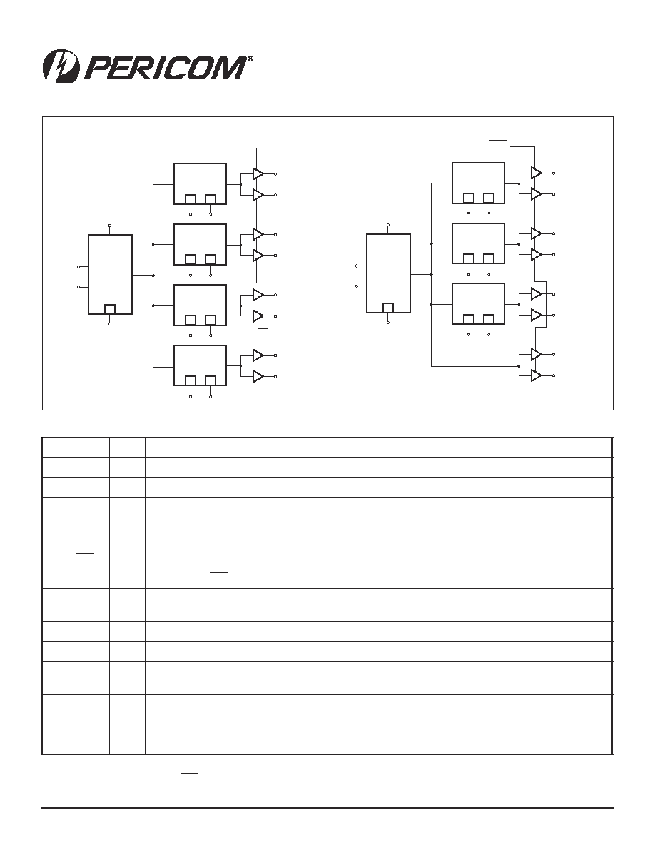
Logic Block Diagrams
PI6C3Q991A
Skew
Select
3
3
3
1F1:0
1Q0
1Q1
Skew
Select
3
3
2F1:0
2Q0
2Q1
Skew
Select
3
3
3F1:0
3Q0
3Q1
Skew
Select
3
3
4F1:0
4Q0
4Q1
GND/sOE
REF
PLL
V
CCQ
/PE
FB
FS
PI6C3Q993A
Skew
Select
3
3
3
1F1:0
1Q0
1Q1
Skew
Select
3
3
2F1:0
2Q0
2Q1
Skew
Select
3
3
3F1:0
3Q0
3Q1
4Q0
4Q1
GND/sOE
REF
PLL
V
CCQ
/PE
FB
FS

12345678901234567890123456789012123456789012345678901234567890121234567890123456789012345678901212345678901234567890123456789012123456789012
12345678901234567890123456789012123456789012345678901234567890121234567890123456789012345678901212345678901234567890123456789012123456789012
PI6C3Q991A, PI6C3Q993A
3.3V Programmable Skew PLL Clock Driver SuperClock
3
PS8628A 02/06/03
Programmable Skew
Output skew with respect to the REF input is adjustable to compen-
sate for PCB trace delays, backplane propagation delays or to
accommodate requirements for special timing relationships between
clocked components. Skew is selectable as a multiple of a time unit
t
U
which is of the order of a nanosecond (see Table 2). There are 9
skew configurations available for each output pair. These configu-
rations are choosen by the nF1:0 control pins. In order to minimize
the number of control pins, 3-level inputs (HIGH-MID-LOW) are
used, they are intended for but not restricted to hard-wiring. Undriven
3-level inputs default to the MID level. Where programmable skew
is not a requirement, the control pins can be left open for the zero skew
default setting. The Skew Selection Table (Table 3) shows how to
select specific skew taps by using the nF1:0 control pins.
External Feedback
By providing external feedback, the PI6C3Q99x family gives users
flexibility with regard to skew adjustment. The FB signal is compared
with the input REF signal at the phase detector in order to drive the
V
CO
. Phase differences cause the V
CO
of the PLL to adjust upwards
or downwards accordingly. An internal loop filter moderates the
response of the V
CO
to the phase detector. The loop filter transfer
function has been chosen to provide minimal jitter (or frequency
variation) while still providing accurate responses to input fre-
quency changes.
W
O
L
=
S
F
D
I
M
=
S
F
H
G
I
H
=
S
F
s
t
n
e
m
m
o
C
t
(
n
o
i
t
a
l
u
c
l
a
c
ti
n
u
g
n
i
m
i
T
U
)
F
x
4
4
(
/
1
M
O
N
)
F
x
6
2
(
/
1
M
O
N
)
F
x
6
1
(
/
1
M
O
N
)
V
O
C
F
(
e
g
n
a
r
y
c
n
e
u
q
e
r
f
M
O
N
)
)
3
,
2
(
z
H
M
5
3
o
t
5
1
z
H
M
0
6
o
t
5
2
z
H
M
0
1
1
o
t
0
4
e
g
n
a
r
t
n
e
m
t
s
u
j
d
a
w
e
k
S
)
4
(
t
n
e
m
t
s
u
j
d
a
.
x
a
M
s
n
9
0
.
9
±
°
9
4
±
%
4
1
±
s
n
3
2
.
9
±
°
3
8
±
%
3
2
±
s
n
8
3
.
9
±
°
5
3
1
±
%
7
3
±
e
m
i
t
e
l
c
y
c
f
o
%
s
e
e
r
g
e
d
e
s
a
h
P
s
n
F
,
1
e
l
p
m
a
x
E
M
O
N
z
H
M
5
1
=
t
U
s
n
2
5
.
1
=
F
,
2
e
l
p
m
a
x
E
M
O
N
z
H
M
5
2
=
t
U
s
n
1
9
.
0
=
t
U
s
n
4
5
.
1
=
F
,
3
e
l
p
m
a
x
E
M
O
N
z
H
M
0
3
=
t
U
s
n
6
7
.
0
=
t
U
s
n
8
2
.
1
=
F
,
4
e
l
p
m
a
x
E
M
O
N
z
H
M
0
4
=
t
U
s
n
6
9
.
0
=
t
U
s
n
6
5
.
1
=
F
,
5
e
l
p
m
a
x
E
M
O
N
z
H
M
0
5
=
t
U
s
n
7
7
.
0
=
t
U
s
n
5
2
.
1
=
F
,
6
e
l
p
m
a
x
E
M
O
N
z
H
M
0
8
=
t
U
s
n
8
7
.
0
=
Table 2. PLL Programmable Skew Range and Resolution Table
Notes:
2. The device may be operated outside recommended frequency ranges without damage, but functional operation is not guaranteed.
Selecting the appropriate FS value based on input frequency range allows the PLL to operate in its `sweet spot' where jitter is
lowest.
3. The level to be set on FS is determined by the nominal operating frequency of the V
CO
and Time Unit Generator. The V
CO
frequency always appears at 1Q1:0, 2Q1:0, and the higher outputs when they are operated in their undivided modes. The
frequency appearing at the REF and FB inputs will be the same as the V
CO
when the output connected to FB is undivided.
The frequency of the REF and FB inputs will be 1/2 or 1/4 the V
CO
frequency when the part is configured for a frequency
multiplication by using a divided output as the FB input.
4. Skew adjustment range assumes that a zero skew output is used for feedback. If a skewed Q output is used for feedback, then
adjustment range will be greater. For example if a 4t
U
skewed output is used for feedback, all other outputs will be skewed
4t
U
in addition to whatever skew value is programmed for those outputs. `Max adjustment' range applies to output pairs
3 and 4 where ±6t
U
skew adjustment is possible and at the lowest F
NOM
value.
12345678901234567890123456789012123456789012345678901234567890121234567890123456789012345678901212345678901234567890123456789012123456789012
12345678901234567890123456789012123456789012345678901234567890121234567890123456789012345678901212345678901234567890123456789012123456789012
PI6C3Q991A, PI6C3Q993A
3.3V Programmable Skew PLL Clock Driver SuperClock
4
PS8628A 02/06/03
0
:
1
F
n
)
2
#
,
1
#
r
i
a
P
(
w
e
k
S
)
3
#
r
i
a
P
(
w
e
k
S
)
4
#
r
i
a
P
(
w
e
k
S
)
5
(
L
L
)
6
(
t
4
U
2
y
b
e
d
i
v
i
D
*
2
y
b
e
d
i
v
i
D
M
L
t
3
U
t
6
U
t
6
U
H
L
t
2
U
t
4
U
t
4
U
L
M
t
1
U
t
2
U
t
2
U
M
M
w
e
k
s
o
r
e
Z
w
e
k
s
o
r
e
Z
w
e
k
s
o
r
e
Z
H
M
t
1
+
U
t
2
+
U
t
2
+
U
L
H
t
2
+
U
t
4
+
U
t
4
+
U
M
H
t
3
+
U
t
6
+
U
t
6
+
U
H
H
t
4
+
U
*
4
y
b
e
d
i
v
i
D
d
e
t
r
e
v
n
I
)
7
(
Table 3. Skew Selection Table for Output Pairs
Supply Voltage to Ground ...................................... 0.5V to 7.0V
Input Voltage .......................................................... 0.5V to 7.0V
Maximum Power Dissipation at T
A
= 85°C, PLCC ....... 0.80 watts
QSOP ....... 0.66 watts
TSTG Storage Temperature .................................. 65°C to 150°C
Table 4. Absolute Maximum Ratings
Table 5. Recommended Operating Range
l
o
b
m
y
S
n
o
i
t
p
i
r
c
s
e
D
A
3
9
9
Q
3
C
6
I
P
/
A
1
9
9
Q
3
C
6
I
P
5
-
A
3
9
9
Q
3
C
6
I
P
/
5
-
A
9
9
Q
3
C
6
I
P
)
l
a
i
r
t
s
u
d
n
I
(
A
3
9
9
Q
3
C
6
I
P
/
A
1
9
9
Q
3
C
6
I
P
2
-
A
3
9
9
Q
3
C
6
I
P
/
2
-
A
1
9
9
Q
3
C
6
I
P
5
-
A
3
9
9
Q
3
C
6
I
P
/
5
-
A
1
9
9
Q
3
C
6
I
P
)
l
a
i
c
r
e
m
m
o
C
(
s
t
i
n
U
.
n
i
M
.
x
a
M
.
n
i
M
.
x
a
M
V
C
C
e
g
a
tl
o
V
y
l
p
p
u
S
r
e
w
o
P
0
.
3
6
.
3
0
.
3
6
.
3
V
T
A
e
r
u
t
a
r
e
p
m
e
T
g
n
it
a
r
e
p
O
t
n
e
i
b
m
A
0
4
5
8
0
0
7
C
°
Stresses above those listed under Absolute Maximum Ratings
may cause permanent damage to the device. These ratings
arestress specifications only and functional operation of the
device at these or any other conditions above those listed in the
operational sections of the specifications is not implied. Expo-
sure to absolute maximum rating conditions for extended periods
may affect product reliability.
Notes:
5. Programmable skew on pair #4 is not applicable for the PI6C3Q993A.
6. LL disables outputs if TEST = MID and GND/sOE = HIGH.
7. When pair #4 is set to HH (inverted), GND/sOE disables pair #4 HIGH when V
CCQ
/PE = HIGH, GND/sOE disables pair #4 LOW
when V
CCQ
/PE = LOW.
* The rising edge of 3Qx and 4Qx are not aligned only when both 3F1 : 0 = HH (divide by 4) and 4F1
:
0 = LL (divide by 2) are
selected. This is not applicable for PI6C3Q993A.

12345678901234567890123456789012123456789012345678901234567890121234567890123456789012345678901212345678901234567890123456789012123456789012
12345678901234567890123456789012123456789012345678901234567890121234567890123456789012345678901212345678901234567890123456789012123456789012
PI6C3Q991A, PI6C3Q993A
3.3V Programmable Skew PLL Clock Driver SuperClock
5
PS8628A 02/06/03
l
o
b
m
y
S
r
e
t
e
m
a
r
a
P
n
o
i
t
i
d
n
o
C
t
s
e
T
.
n
i
M
.
x
a
M
s
t
i
n
U
V
H
I
e
g
a
tl
o
V
H
G
I
H
t
u
p
n
I
H
G
I
H
c
i
g
o
L
d
e
e
t
n
a
r
a
u
G
)
y
l
n
o
s
t
u
p
n
i
B
F
,
F
E
R
(
0
.
2
5
.
5
V
V
L
I
e
g
a
tl
o
V
W
O
L
t
u
p
n
I
W
O
L
c
i
g
o
L
d
e
e
t
n
a
r
a
u
G
)
y
l
n
o
s
t
u
p
n
i
B
F
,
F
E
R
(
5
.
0
8
.
0
V
H
H
I
e
g
a
tl
o
V
H
G
I
H
t
u
p
n
I
)
8
(
y
l
n
O
s
t
u
p
n
I
l
e
v
e
L
-
3
V
C
C
6
.
0
V
M
M
I
e
g
a
tl
o
V
D
I
M
t
u
p
n
I
)
8
(
y
l
n
O
s
t
u
p
n
I
l
e
v
e
L
-
3
V
C
C
2
/
3
.
0
V
C
C
3
.
0
+
2
/
V
L
L
I
e
g
a
tl
o
V
W
O
L
t
u
p
n
I
)
8
(
y
l
n
O
s
t
u
p
n
I
l
e
v
e
L
-
3
6
.
0
I
N
I
)
y
l
n
o
s
t
u
p
n
i
B
F
,
F
E
R
(
t
n
e
r
r
u
C
e
g
a
k
a
e
L
t
u
p
n
I
V
N
I
V
=
C
C
,
D
N
G
r
o
V
C
C
.
x
a
M
=
5
A
µ
I
3
)
0
:
1
F
n
,
S
F
,
T
S
E
T
(
t
n
e
r
r
u
C
C
D
t
u
p
n
I
l
e
v
e
L
-
3
V
N
I
V
=
C
C
V
N
I
V
=
C
C
2
/
V
N
I
D
N
G
=
l
e
v
e
L
H
G
I
H
l
e
v
e
L
D
I
M
l
e
v
e
L
W
O
L
0
0
2
0
5
0
0
2
I
U
P
V
(
t
n
e
r
r
u
C
p
U
-l
l
u
P
t
u
p
n
I
Q
C
C
)
E
P
/
V
C
C
V
,.
x
a
M
=
N
I
D
N
G
=
0
0
1
I
D
P
)
E
O
s
/
D
N
G
(
t
n
e
r
r
u
C
n
w
o
D
-l
l
u
P
t
u
p
n
I
V
C
C
V
,.
x
a
M
=
N
I
V
=
C
C
0
0
1
V
H
O
e
g
a
tl
o
V
H
G
I
H
t
u
p
t
u
O
V
C
C
I
,.
n
i
M
=
H
O
=
A
m
2
1
2
.
2
V
V
L
O
e
g
a
tl
o
V
W
O
L
t
u
p
t
u
O
V
C
C
I
,.
n
i
M
=
L
O =
A
m
2
1
5
5
.
0
Table 6. DC Characteristics Over Operating Range
l
o
b
m
y
S
r
e
t
e
m
a
r
a
P
n
o
i
t
i
d
n
o
C
t
s
e
T
.
p
y
T
.
x
a
M
s
t
i
n
U
I
Q
C
C
t
n
e
r
r
u
C
y
l
p
p
u
S
r
e
w
o
P
t
n
e
c
s
e
i
u
Q
V
C
C
,
W
O
L
=
F
E
R
,.
d
i
M
=
T
S
E
T
,.
x
a
M
=
d
e
d
a
o
l
n
u
s
t
u
p
t
u
o
ll
A
,
W
O
L
=
E
O
s
/
D
N
G
0
.
8
5
1
A
m
I
C
C
H
G
I
H
t
u
p
n
I
r
e
p
t
n
e
r
r
u
C
y
l
p
p
u
S
r
e
w
o
P
)
9
(
V
C
C
V
,.
x
a
M
=
N
I
V
0
.
3
=
0
.
1
0
3
A
µ
I
D
C
C
t
u
p
t
u
O
r
e
p
t
n
e
r
r
u
C
y
l
p
p
u
S
r
e
w
o
P
c
i
m
a
n
y
D
)
9
(
V
C
C
C
,.
x
a
M
=
L
F
p
0
=
5
5
0
9
/
A
µ
z
H
M
I
C
t
n
e
r
r
u
C
y
l
p
p
u
S
r
e
w
o
P
l
a
t
o
T
)
9
(
V
C
C
F
,
V
3
.
3
=
F
E
R
C
,
z
H
M
0
2
=
L
F
p
0
6
1
=
)
0
1
(
9
2
A
m
I
C
t
n
e
r
r
u
C
y
l
p
p
u
S
r
e
w
o
P
l
a
t
o
T
)
9
(
V
C
C
F
,
V
3
.
3
=
F
E
R
C
,
z
H
M
3
3
=
L
F
p
0
6
1
=
)
0
1
(
2
4
I
C
t
n
e
r
r
u
C
y
l
p
p
u
S
r
e
w
o
P
l
a
t
o
T
)
9
(
V
C
C
F
,
V
3
.
3
=
F
E
R
C
,
z
H
M
6
6
=
L
F
p
0
6
1
=
)
0
1
(
6
7
Table 7. Power Supply Characteristics
Notes:
8. These inputs are normally wired to V
CC
, GND, or unconnected. Internal termination resistors bias unconnected inputs to V
CC
/2.
If these inputs are switched, the function and timing of the outputs may glitched, and the PLL may require an additional t
LOCK
time before all datasheet limits are achieved.
9. Guaranteed by characterization but not production tested.
10. For 8 outputs each loaded with 20pF.
N
125