
1
PS7038B 09/08/97
Pin Name Pin # I/O Description
S0
6
I
Select 0, internal pull-up
S1
7
I
Select 1, internal pull-up
X1
2
C
Crystal or clock input, 8 to 23 MHz
X2
3
C
Crystal connection or no connect
CLK
5
O
Clock output
OE
1
I
OE = 1 Enable CLK output
OE = 0 Disable CLK output
3.3V Precision Clock Generator
12345678901234567890123456789012123456789012345678901234567890121234567890123456789012345678901212345678901234567890123456789012123456789012
12345678901234567890123456789012123456789012345678901234567890121234567890123456789012345678901212345678901234567890123456789012123456789012
PI6C918/919
Features
∑ No external capacitors (919 only)
∑ Excellent signal quality
∑ Very low jitter
∑ Precise frequencies
∑ Minimal undershoot, ringback or overshoot
∑ Nearly perfect 50% duty cycle
∑ Four selectable clock frequencies
∑ Operates at Vcc = 3.3V
∑ Output may be disabled to save power
∑ Small 150-mil wide SOIC -8 (W8) package
saves board area
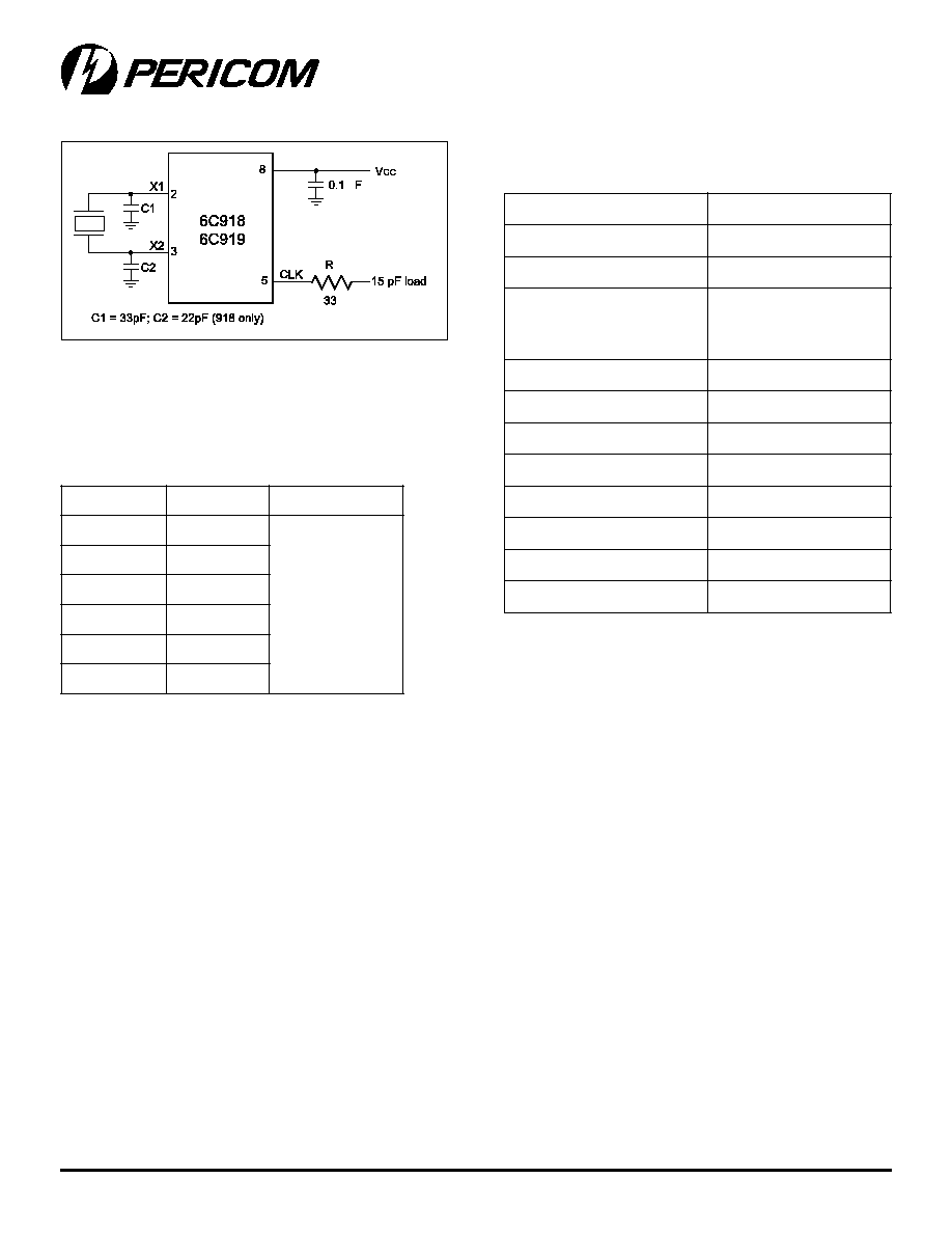
Pin Configuration
Pin Description
Product Speed Grades
Max CLK
Max VCO
Part No.
Output Freq.
Frequency
PI6C918/919
80 MHz
160 MHz
PI6C918A/919A
100 MHz
200 MHz
PI6C918B/919B
120 MHz
240 MHz
Output CLK Frequency Selection
Vcc
1
OE
8
S1
2
X1
7
S0
3
X2
6
CLK
4
GND
5
8-PIN
W8
Note:
1. I = Input, O = Output, C = Crystal
Description
The PI6C918 and PI6C919 are high-precision, low-voltage
general-purpose clock generators that reach a maximum output
frequency of 120 MHz. These devices use an external low-cost
crystal to generate very accurate and stable system clocks.
These frequency synthesizers include a crystal oscillator, a
programmable PLL and an output buffer. Any one of four
different output frequencies can be selected via two select pins
(S0, S1). The frequency multipliers are: 2, 4, 5, and 7.
The PI6C919 has on-chip capacitors, eliminating the need for
external capacitors at the X1, X2 pins. This reduces overall parts
count and board area, and increases reliability.
The OE (output enable) pin may be pulled down to disable the
output buffer and save system power.
The small surface-mount SOIC-8 package is ideal for compact
portable equipment applications.
Notes:
1. Indicates popular target frequencies.
2. The ratio of N/M may be changed by mask option.
n
o
i
t
c
e
l
e
S
0
S
,
1
S
M
/
N
)
2
(
k
c
o
l
C
0
1
g
n
i
s
u
(
)
l
a
t
X
z
H
M
k
c
o
l
C
6
.
6
1
g
n
i
s
u
(
)
l
a
t
X
z
H
M
k
c
o
l
C
0
2
g
n
i
s
u
(
)
l
a
t
X
z
H
M
k
c
o
l
C
1
.
2
2
g
n
i
s
u
(
)
l
a
t
X
z
H
M
0
0
2
≠
3
.
3
3
)
1
(
0
4
2
.
4
4
1
0
4
0
4
)
1
(
6
.
6
6
)
1
(
0
8
)
1
(
4
.
8
8
0
1
5
0
5
)
1
(
3
8
0
0
1
)
1
(
5
.
0
1
1
1
1
7
0
7
)
1
(
6
1
1
≠
≠
2
PS7038B 09/08/97
12345678901234567890123456789012123456789012345678901234567890121234567890123456789012345678901212345678901234567890123456789012123456789012
PI6C918/919
3.3V Precision Clock Generator
Storage Temperature ................................................................. ≠65∞C to +150∞C
Ambient Temperature with Power Applied .................................... 0∞C to +70∞C
Supply Voltage to Ground Potential (Inputs & Vcc Only) .......... ≠0.5V to +7.0V
Supply Voltage to Ground Potential (Outputs & D/O Only) ....... ≠0.5V to +7.0V
DC Input Voltage ......................................................................... ≠0.5V to +7.0V
DC Output Current ................................................................................... 120 mA
Power Dissipation ......................................................................................... 0.5W
Note:
Stresses greater than those listed under
MAXIMUM RATINGS may cause perma-
nent damage to the device. This is a stress
rating only and functional operation of the
device at these or any other conditions above
those indicated in the operational sections of
this specification is not implied. Exposure
to absolute maximum rating conditions for
extended periods may affect reliability.
DC Electrical Characteristics
Operating Range, V
CC
= 3.3V ±10% (918/919/918A/919A). Vcc = 3.3V ±5% (918B/919B), Temperature 0∞C to +70∞C
Symbol
Description
Test Conditions
(1)
Min.
Typ.
Max.
Units
d
T
Duty Cycle,
V
TH
= 1.4V
45
50
55
%
T
r
, T
f
Rise/Fall Time
20% and 80% Vcc
--
--
3
ns
t
PU
Power-up Time
(2)
--
--
10
ms
F
XTAL
Crystal Input Frequency
918/918A/919/919A
10
--
20
MHz
918B/919B
10
--
24
Tj1s
One Sigma Jitter
f
VCO
60 MHz
--
--
60
ps
Note:
1. Test load of 15 pF, 2-inch trace
2. Time from when the power supply reaches 90% until locked clock output waveform is reached.
Maximum Ratings
Note: 1. There is no guarantee that on-chip capacitance eliminates the need for external capacitors.
AC Electrical Characteristics
Operating Range, V
CC
= 3.3V ±10% (918/919/918A/919A). Vcc = 3.3V ±5% (918B/919B), Temperature 0∞C to +70∞C
l
o
b
m
y
S
n
o
i
t
p
i
r
c
s
e
D
s
n
o
i
t
i
d
n
o
C
t
s
e
T
.
n
i
M
.
p
y
T
.
x
a
M
s
t
i
n
U
V
H
O
e
g
a
t
l
o
V
H
G
I
H
t
u
p
t
u
O
V
,
.
n
i
M
=
c
c
V
N
I
V
=
H
I
V
r
o
L
I
V
H
O
A
m
8
-
=
V
C
C
4
.
0
-
-
-
V
V
L
O
e
g
a
t
l
o
V
W
O
L
t
u
p
t
u
O
V
L
O
A
m
8
=
-
-
4
.
0
V
H
I
e
g
a
t
l
o
V
H
G
I
H
t
u
p
n
I
t
c
e
l
e
S
V
C
C
V
5
=
0
.
2
-
-
V
L
I
e
g
a
t
l
o
V
W
O
L
t
u
p
n
I
t
c
e
l
e
S
-
-
8
.
0
V
H
I
t
n
e
r
r
u
C
H
G
I
H
t
u
p
n
I
t
c
e
l
e
S
V
C
C
V
,
.
x
a
M
=
N
I
= V
C
C
-
-
5
µ
A
V
L
I
t
n
e
r
r
u
C
W
O
L
t
u
p
n
I
t
c
e
l
e
S
V
C
C
V
,
.
x
a
M
=
N
I
V
0
=
-
-
0
1
-
I
C
C
t
n
e
r
r
u
C
y
l
p
p
u
S
V
C
C
z
H
M
0
4
=
y
c
n
e
u
q
e
r
f
K
L
C
,
.
x
a
M
=
-
0
1
0
2
A
m
L
R
e
c
n
a
t
s
i
s
e
R
e
v
i
t
a
g
e
N
2
X
,
1
X
0
0
0
,
1
-
0
0
0
,
2
-
-
R
B
F
l
a
n
r
e
t
n
I
2
X
,
1
X
p
i
h
c
-
n
O
e
c
n
a
t
s
i
s
e
R
k
c
a
b
d
e
e
F
7
2
2
-
-
k
3
PS7038B 09/08/97
12345678901234567890123456789012123456789012345678901234567890121234567890123456789012345678901212345678901234567890123456789012123456789012
PI6C918/919
3.3V Precision Clock Generator
Notes:
a. Locate crystal as close to X1, X2 pins as possible.
b. Connect a 0.1
µ
F bypass capacitor at Vcc (Pin 8).
External Circuit
Pericom Semiconductor Corporation
2380 Bering Drive ∑ San Jose, CA 95131 ∑ 1-800-435-2336 ∑ Fax (408) 435-1100 ∑ http://www.pericom.com
Ordering Information
Crystal Specifications
It is the customer's responsibility to procure the prototype and
production crystals directly from crystal vendors.
µ
.
o
N
t
r
a
P
.
q
e
r
F
.
x
a
M
e
g
a
k
c
a
P
W
8
1
9
C
6
I
P
z
H
M
0
8
8
-
C
I
O
S
w
o
r
r
a
N
W
A
8
1
9
C
6
I
P
z
H
M
0
0
1
W
B
8
1
9
C
6
I
P
z
H
M
0
2
1
W
9
1
9
C
6
I
P
z
H
M
0
8
W
A
9
1
9
C
6
I
P
z
H
M
0
0
1
W
B
9
1
9
C
6
I
P
z
H
M
0
2
1
c
i
t
s
i
r
e
t
c
a
r
a
h
C
l
a
c
i
p
y
T
)
1
(
e
u
l
a
V
F
,
y
c
n
e
u
q
e
r
F
l
a
n
i
m
o
n
z
H
M
0
0
2
3
4
.
8
1
C
∞
5
2
t
a
e
c
n
a
r
e
l
o
T
y
c
n
e
u
q
e
r
F
m
p
p
0
5
±
y
t
i
l
i
b
a
t
S
y
c
n
e
u
q
e
r
F
e
r
u
t
a
r
e
p
m
e
T
.
s
v
g
n
i
g
A
.
s
v
)
C
∞
0
7
o
t
C
∞
0
(
m
p
p
5
3
±
s
r
a
e
y
4
/
m
p
p
5
1
±
e
d
o
M
n
o
i
t
a
l
l
i
c
s
O
l
a
t
n
e
m
a
d
n
u
F
e
d
o
M
n
o
i
t
a
r
b
i
l
a
C
t
n
a
n
o
s
e
r
l
e
l
l
a
r
a
P
C
,
e
c
n
a
t
i
c
a
p
a
C
d
a
o
L
L
l
a
t
n
e
m
a
d
n
u
F
,
F
p
0
2
C
,
e
c
n
a
t
i
c
a
p
a
C
t
n
u
h
S
O
l
a
t
n
e
m
a
d
n
u
F
,
.
x
a
m
F
p
7
1
R
,
e
c
n
a
t
s
i
s
e
R
s
e
i
r
e
S
0
5
l
a
c
i
p
y
T
l
e
v
e
L
e
v
i
r
D
1m
l
a
c
i
p
y
T
e
r
u
t
a
r
e
p
m
e
T
g
n
i
t
a
r
e
p
O
C
∞
0
7
o
t
∞
0
e
r
u
t
a
r
e
p
m
e
T
e
g
a
r
o
t
S
C
∞
5
8
o
t
∞
0
4
-