1
PS8353A 11/23/98
Product Description
Pericom Semiconductors PI74ALVTC series of logic circuits are
produced in the Companys advanced 0.35 micron CMOS tech-
nology, achieving industry leading speed.
The PI74ALVTC16240 buffer/driver is designed specifically to
improve both the performance and density of 3-state memory
address drivers, clock drivers, and bus-oriented receivers and
transmitters.
The device can be used as four 4-bit buffers, two 8-bit buffers, or
one 16-bit buffer. It provides inverting outputs and symmetrical
active-low output-enable (OE) inputs.
To ensure the high-impedance state during power up or power
down, OE should be tied to Vdd through a pullup resistor; the
minimum value of the resistor is determined by the current-sink-
ing capability of the driver.
The family offers both I/O Tolerant, which allows it to operate in
mixed 1.8/3.6V systems, and Bus Hold, which retains the data
inputs last state whenever the data input goes to high-impedance,
preventing floating inputs and eliminating the need for pullup/
down resistors.
12345678901234567890123456789012123456789012345678901234567890121234567890123456789012345678901212345678901234567890123456789012123456789012
12345678901234567890123456789012123456789012345678901234567890121234567890123456789012345678901212345678901234567890123456789012123456789012
Product Features
PI74ALVTC family is designed for low voltage operation,
V
DD
= 1.8V to 3.6V
Supports Live Insertion
3.6V I/O Tolerant Inputs and Outputs
Bus Hold
High Drive, -32/64mA @ 3.3V
Uses patented noise reduction circuitry
Power-off high impedance inputs and outputs
Industrial operation at 40�C to +85�C
Packages available:
48-pin 240 mil wide plastic TSSOP (A)
48-pin 173 mil wide plastic TVSOP (K)
48-pin 300 mil wide plastic SSOP (V)
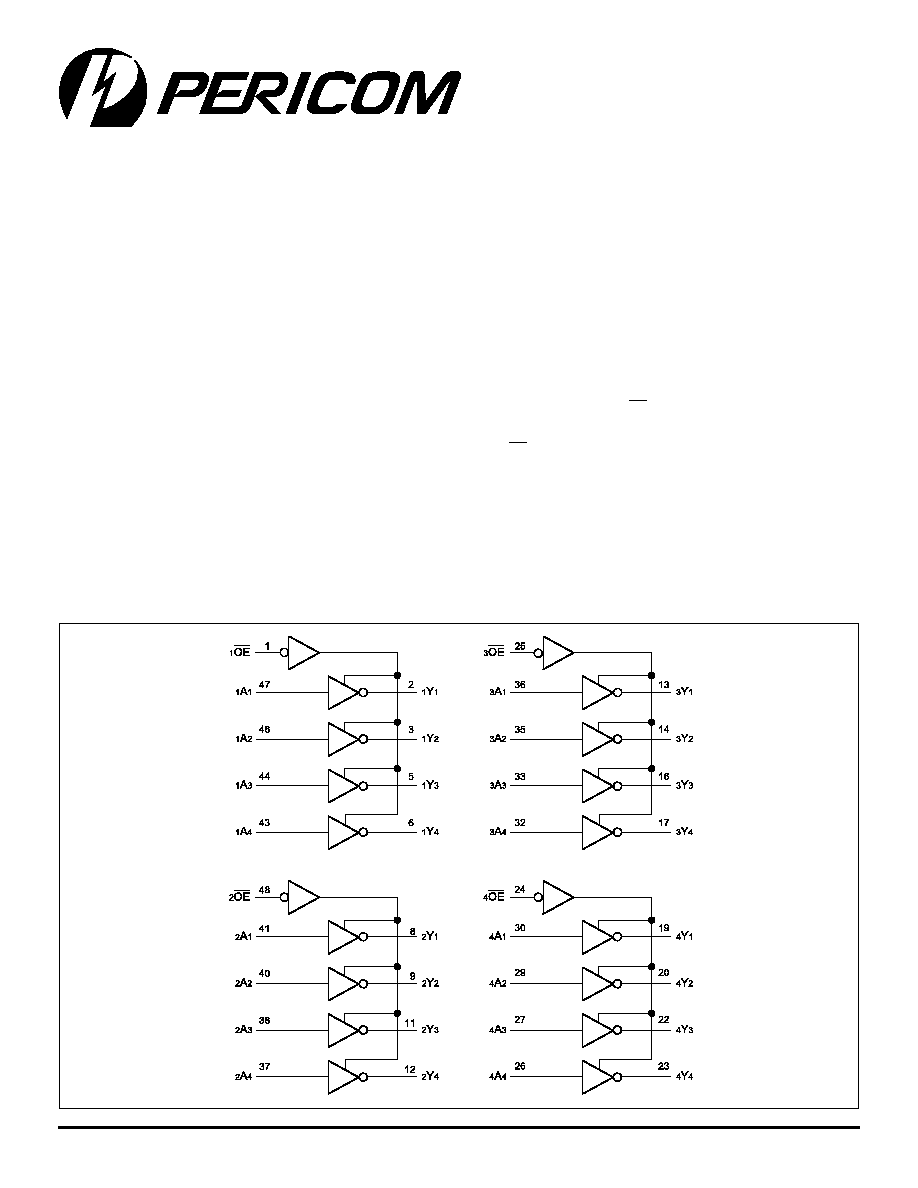
PI74ALVTC16240
16-Bit Buffer/Driver
with 3-State Outputs
Logic Block Diagram
2
PS8353A 11/23/98
12345678901234567890123456789012123456789012345678901234567890121234567890123456789012345678901212345678901234567890123456789012123456789012
PI74ALVTC16240
16-Bit Buffer Driver With 3-State Outputs
s
t
u
p
n
I
s
t
u
p
t
u
O
E
O
n
A
n
X
x
Y
n
L
H
L
L
L
H
H
X
Z
1
2
3
4
5
6
7
8
9
48
10
47
11
46
12
45
13
44
14
43
15
42
16
41
17
40
18
39
19
38
20
37
21
36
22
35
23
34
24
33
32
31
30
29
28
27
26
25
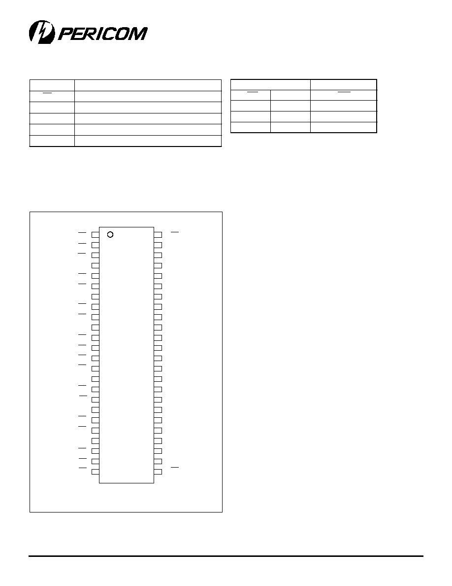
Pin Name
Description
nOE
3-State Output Enable Inputs (Active LOW)
nAx
Inputs
nYx
3-State Outputs
GND
Ground
V
CC
Power
Product Pin Description
Truth Table
(1)
Notes:
1.
H = High Signal Level
L = Low Signal Level
X = Don't Care or Irrelevant
Z = High Impedance
Product Pin Configuration
1
OE
1
Y
1
1
Y
2
GND
1
Y
3
1
Y
4
V
CC
2
Y
1
2
Y
2
GND
2
Y
3
2
Y
4
3
Y
1
3
Y
2
GND
3
Y
3
3
Y
4
V
CC
4
Y
1
4
Y
2
GND
4
Y
3
4
Y
4
4
OE
2
OE
1
A
1
1
A
2
GND
1
A
3
1
A
4
V
CC
2
A
1
2
A
2
GND
2
A
3
2
A
4
3
A
1
3
A
2
GND
3
A
3
3
A
4
V
CC
4
A
1
4
A
2
GND
4
A
3
4
A
4
3
OE
48-PIN
A48
K48
V48
3
PS8353A 11/23/98
12345678901234567890123456789012123456789012345678901234567890121234567890123456789012345678901212345678901234567890123456789012123456789012
PI74ALVTC16240
16-Bit Buffer Driver With 3-State Outputs
Stresses greater than those listed under MAXIMUM
RATINGS may cause permanent damage to the device.
This is a stress rating only and functional operation of the
device at these or any other conditions above those indi-
cated in the operational sections of this specification is not
implied. Exposure to absolute maximum rating conditions
for extended periods may affect reliability.
Supply Voltage Range, V
DD
.......................................... 0.5V to 4.6V
Input Voltage Range, V
I
................................................. -0.5V to 4.6V
Output Voltage Range, V
O
(3-Stated) ............................ -0.5V to 4.6V
Output Voltage Range, V
O
(1)
(Active) ................. 0.5V to V
DD
+0.5V
DC Input Diode Current (I
IK
) V
I
<0V........................................ -50mA
DC Output Diode Current (I
OK
)
V
O
<0V ................................................................................... -50mA
V
O
>V
DD
................................................................................ �50mA
DC Output Source/Sink Current (I
OH
/I
OL
) ......................... -64/128mA
DC V
DD
or GND Current per Supply Pin (I
CC
or GND) ....... �100mA
Storage Temperature Range, T
stg
................................. 65�C to150�C
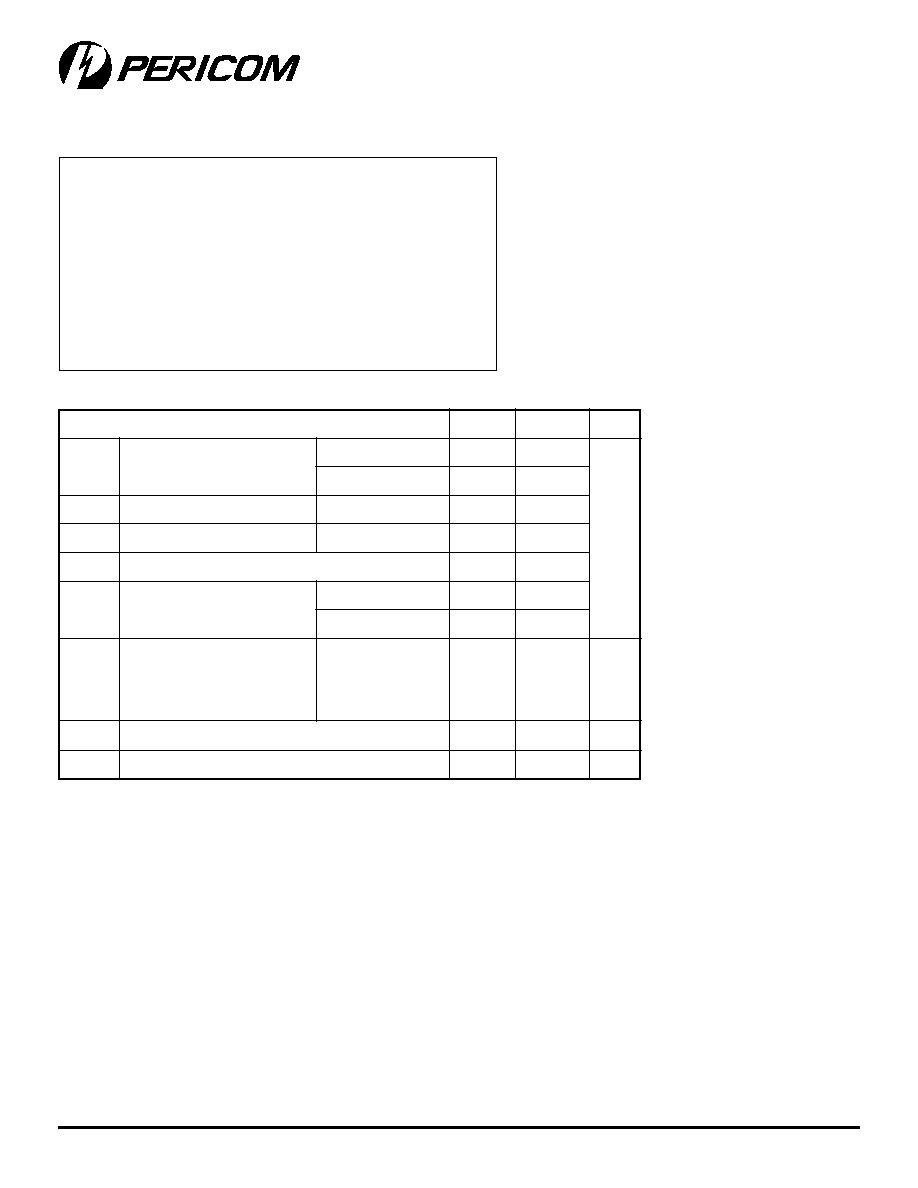
Recommended Operating Conditions
2
Maximum Ratings
(Above which the useful life may be impaired. For user guidelines, not tested.)
Notes
1. Absolute maximum of I
O
must be observed.
2. Unused control inputs must be held HIGH or LOW to prevent them from floating.
3 As measured between 0.8V and 2.0V, V
DD
= 3.0V.
.
n
i
M
.
x
a
M
s
ti
n
U
V
D
D
e
g
a
tl
o
v
y
l
p
p
u
S
g
n
it
a
r
e
p
O
8
.
1
6
.
3
V
y
l
n
O
n
o
it
n
e
t
e
R
a
t
a
D
2
.
1
6
.
3
V
H
I
e
g
a
tl
o
v
t
u
p
n
i
l
e
v
el
-
h
g
i
H
V
D
D
V
6
.
3
o
t
V
7
.
2
=
0
.
2
V
L
I
e
g
a
tl
o
v
t
u
p
n
i
l
e
v
el
-
w
o
L
V
D
D
V
6
.
3
o
t
V
7
.
2
=
8
.
0
V
I
e
g
a
tl
o
v
t
u
p
n
I
3
.
0
-
6
.
3
V
O
e
g
a
tl
o
v
t
u
p
t
u
O
e
t
a
t
S
e
v
it
c
A
0
V
D
D
e
t
a
t
S
ff
O
0
6
.
3
I
n
i
t
n
e
rr
u
c
t
u
p
t
u
O
H
O
I/
L
O
V
D
D
V
6
.
3
o
t
V
0
.
3
=
V
D
D
V
6
.
3
o
t
V
0
.
3
=
V
D
D
V
7
.
2
o
t
V
3
.
2
=
V
D
D
V
8
.
1
=
4
6
/
2
3
-
4
2
�
8
1
�
6
�
A
m
D /tDv
e
t
a
r
ll
a
f
r
o
e
si
r
n
o
it
si
s
n
a
rt
t
u
p
n
I
)
3
(
0
0
1
V
/
s
n
T
A
e
r
u
tr
e
p
m
e
t
ri
a
-
e
e
rf
g
n
it
a
r
e
p
O
- 0
4
5
8
C

4
PS8353A 11/23/98
12345678901234567890123456789012123456789012345678901234567890121234567890123456789012345678901212345678901234567890123456789012123456789012
PI74ALVTC16240
16-Bit Buffer Driver With 3-State Outputs
r
e
t
e
m
a
r
a
P
s
n
o
it
i
d
n
o
C
V
D
D
.
n
i
M
.
p
y
T
.
x
a
M
s
ti
n
U
V
H
I
e
g
a
tl
o
V
t
u
p
n
I
l
e
v
e
L
H
G
I
H
6
.
3
-
7
.
2
0
.
2
V
V
L
I
e
g
a
tl
o
V
t
u
p
n
I
l
e
v
e
L
W
O
L
8
.
0
V
H
O
e
g
a
tl
o
V
t
u
p
t
u
O
l
e
v
e
L
H
G
I
H
I
H
O
= - 0
0
1 mA
V
D
D
2
.
0
-
I
H
O
= -
A
m
2
1
7
.
2
2
.
2
I
H
O
= -
A
m
8
1
0
.
3
4
.
2
I
H
O
= -
A
m
4
2
2
.
2
I
H
O
= -
A
m
2
3
0
.
2
V
L
O
e
g
a
tl
o
V
t
u
p
t
u
O
l
e
v
e
L
W
O
L
I
L
O
=
0
0
1 mA
6
.
3
-
7
.
2
2
.
0
I
L
O
= 2
1 A
m
7
.
2
4
.
0
I
L
O
= 8
1 A
m
0
.
3
4
.
0
I
L
O
= 4
2 A
m
5
4
.
0
I
L
O
= 2
3 A
m
5
.
0
I
L
O
= 4
6 A
m
5
5
.
0
I
I
t
n
e
rr
u
C
e
g
a
k
a
e
L
t
u
p
n
I
V
I
V
=
D
D
D
N
G
r
o
,
6
.
3
0
.
5
�
mA
I
Z
O
e
g
a
k
a
e
L
t
u
p
t
u
O
E
T
A
T
S
-
3
V
O
V
6
.
3
=
7
.
2
0
1
�
I
F
F
O
t
n
e
rr
u
C
e
g
a
k
a
e
L
F
F
O
-r
e
w
o
P
V
I
V
r
o
O
�
V
6
.
3
0
0
1
I
L
D
O
w
o
L
t
n
e
rr
u
C
t
u
p
t
u
O
V
IN
= V
IH
V
r
o
IL
,
V
5
.
1
=
o
V
)
1
(
6
.
3
0
5
1
4
3
3
A
m
I
H
D
O
h
g
i
H
t
n
e
rr
u
C
t
u
p
t
u
O
V
IN
= V
IH
V
r
o
IL
,
V
5
.
1
=
o
V
)
1
(
8
5
-
4
1
1
-
I
D
L
O
H
t
n
e
rr
u
C
d
l
o
H
s
u
B
st
u
p
t
u
O
B
r
o
A
V
I
V
8
.
0
=
0
.
3
5
7
mA
V
I
V
0
.
2
=
5
7
-
V
I
V
6
.
3
o
t
0
=
6
.
3
0
0
5
�
I
D
D
t
n
e
rr
u
C
y
l
p
p
u
S
t
n
e
c
s
ei
u
Q
V
I
V
=
D
D
D
N
G
r
o
6
.
3
-
7
.
2
0
5
V
D
D
� V
(
I
V
,
O
) �
V
6
.
3
0
5
�
DI
D
D
I
n
i
e
s
a
e
r
c
n
I
D
D
t
u
p
n
i
r
e
p
V
H
I
V
=
D
D
,
V
6
.
0
-
V
t
a
st
u
p
n
i
r
e
h
t
O
D
D
d
n
G
r
o
0
0
4
Electrical Characteristics over Recommended Operating Free-Air Temperature Range
(unless otherwise noted)
DC Characteristics (2.7V<V
DD
3.6V)
Notes
1. Duration of test must not exceed 1 second with only 1 output tested at a time.

5
PS8353A 11/23/98
12345678901234567890123456789012123456789012345678901234567890121234567890123456789012345678901212345678901234567890123456789012123456789012
PI74ALVTC16240
16-Bit Buffer Driver With 3-State Outputs
DC Characteristics (2.3V<V
DD
2.7V)
Notes:
1. Not Guaranteed
2. Duration of test must not exceed 1 second with only 1 output tested at a time.
Electrical Characteristics over Recommended Operating Free-Air Temperature Range
(unless otherwise noted)
n
o
it
p
i
r
s
s
e
D
s
r
e
t
e
m
a
r
a
P
s
n
o
it
i
d
n
o
C
V
D
D
.
n
i
M
.
p
y
T
.
x
a
M
s
ti
n
U
V
H
I
e
g
a
tl
o
V
t
u
p
n
I
l
e
v
e
L
H
G
I
H
7
.
2
-
3
.
2
6
.
1
V
V
L
I
e
g
a
tl
o
V
t
u
p
n
I
l
e
v
e
L
W
O
L
7
.
0
V
H
O
e
g
a
tl
o
V
t
u
p
t
u
O
l
e
v
e
L
H
G
I
H
I
H
O
0
0
1
-
=
mA
V
D
D
2
.
0
-
I
H
O
A
m
2
1
-
=
3
.
2
8
.
1
I
H
O
A
m
8
1
-
=
7
.
1
V
L
O
e
g
a
tl
o
V
t
u
p
t
u
O
l
e
v
e
L
W
O
L
I
L
O
0
0
1
=
mA
7
.
2
-
3
.
2
2
.
0
I
L
O
A
m
2
1
=
3
.
2
4
.
0
I
L
O
A
m
8
1
=
5
.
0
I
L
O
A
m
4
2
=
5
5
.
0
I
I
t
n
e
r
r
u
C
e
g
a
k
a
e
L
t
u
p
n
I
V
1
V
=
D
D
D
N
G
r
o
7
.
2
0
.
5
�
mA
I
Z
O
e
g
a
k
a
e
L
t
u
p
t
u
O
E
T
A
T
S
-
3
V
O
6
.
3
=
V
3
.
2
0
1
�
I
F
F
O
t
n
e
r
r
u
C
e
g
a
k
a
e
L
F
F
O
-
r
e
w
o
P
V
I
V
r
o
O
6
.
3
�
V
0
0
1
I
L
D
O
w
o
L
t
n
e
r
r
u
C
t
u
p
t
u
O
V
N
I
= V
H
I
r
o V
,
L
I
V
O
V
5
.
1
=
)
2
(
7
.
2
0
1
1
4
6
2
A
m
I
H
D
O
h
g
i
H
t
n
e
r
r
u
C
t
u
p
t
u
O
V
N
I
= V
H
I
r
o V
,
L
I
V
O
V
5
.
1
=
)
2
(
0
3
-
0
6
-
I
D
L
O
H
)
1
(
t
n
e
r
r
u
C
d
l
o
H
s
u
B
s
t
u
p
t
u
O
B
r
o
A
V
I
V
7
.
0
=
5
.
2
0
9
mA
V
I
V
7
.
1
=
0
9
-
I
D
D
t
n
e
r
r
u
C
y
l
p
p
u
S
t
n
e
c
s
e
i
u
Q
V
I
V
=
D
D
D
N
G
r
o
7
.
2
-
3
.
2
0
2
V
D
D
� V
(
I
V
,
O
) �
V
6
.
3
0
2
�
I
D
D
D
n
i
e
s
a
e
r
c
n
I
I
D
D
t
u
p
n
i
r
e
p
V
H
I
V
=
D
D
,
V
6
.
0
-
V
t
a
s
t
u
p
n
I
D
D
d
n
G
r
o
D
B
T

6
PS8353A 11/23/98
12345678901234567890123456789012123456789012345678901234567890121234567890123456789012345678901212345678901234567890123456789012123456789012
PI74ALVTC16240
16-Bit Buffer Driver With 3-State Outputs
DC Characteristics (1.8V<V
DD
2.3V)
Notes:
1. Not Guaranteed
2. Duration of test must not exceed 1 second with only 1 output tested at a time.
Electrical Characteristics over Recommended Operating Free-Air Temperature Range
(unless otherwise noted)
n
o
it
p
i
r
c
s
e
D
s
r
e
t
e
m
a
r
a
P
s
n
o
it
i
d
n
o
C
V
D
D
.
n
i
M
.
p
y
T
.
x
a
M
s
ti
n
U
V
H
I
e
g
a
tl
o
V
t
u
p
n
I
l
e
v
e
L
H
G
I
H
3
.
2
-
8
.
1
x
7
.
0
V
D
D
V
V
L
I
e
g
a
tl
o
V
t
u
p
n
I
l
e
v
e
L
W
O
L
V
x
2
.
0
D
D
V
H
O
e
g
a
tl
o
V
t
u
p
t
u
O
l
e
v
e
L
H
G
I
H
I
H
O
0
0
1
-
=
mA
8
.
1
V
D
D
2
.
0
-
I
H
O
A
m
6
-
=
4
.
1
V
L
O
e
g
a
tl
o
V
t
u
p
t
u
O
l
e
v
e
L
W
O
L
I
L
O
0
0
1
=
mA
2
.
0
I
L
O
A
m
6
=
3
.
0
I
I
t
n
e
rr
u
C
e
g
a
k
a
e
L
t
u
p
n
I
V
I
V
=
D
D
D
N
G
r
o
3
.
2
0
.
5
�
mA
I
Z
O
e
g
a
k
a
e
L
t
u
p
t
u
O
E
T
A
T
S
-
3
V
O
6
.
3
=
V
8
.
1
0
1
�
I
F
F
O
t
n
e
rr
u
C
e
g
a
k
a
e
L
F
F
O
-r
e
w
o
P
V
I
V
=
O
6
.
3
�
V
0
0
1
I
L
D
O
w
o
L
t
n
e
rr
u
C
t
u
p
t
u
O
V
N
I
= V
H
I
r
o V
,
L
I
V
O
=
V
9
.
0
)
2
(
8
.
1
0
5
7
3
1
A
m
I
H
D
O
h
g
i
H
t
n
e
rr
u
C
t
u
p
t
u
O
V
N
I
= V
H
I
r
o V
,
L
I
V
O
=
V
9
.
0
)
2
(
4
1
-
4
3
-
I
D
L
O
H
)
1
(
t
n
e
rr
u
C
d
l
o
H
s
u
B
st
u
p
t
u
O
B
r
o
A
V
I
4
.
0
=
8
.
1
0
5
mA
V
I
3
.
1
=
0
5
-
I
D
D
t
n
e
rr
u
C
y
l
p
p
u
S
t
n
e
c
s
ei
u
Q
V
I
V
=
D
D
D
N
G
r
o
0
2
V
D
D
� V
(
I
V
,
O
) �
V
6
.
3
0
2
�
I
D
D
D
n
i
e
s
a
e
r
c
n
I
I
D
D
t
u
p
n
i
r
e
p
V
I
V
=
D
D
,
V
6
0
-
V
t
a
st
u
p
n
i
r
e
h
t
O
D
D
D
N
G
r
o
0
0
4
7
PS8353A 11/23/98
12345678901234567890123456789012123456789012345678901234567890121234567890123456789012345678901212345678901234567890123456789012123456789012
PI74ALVTC16240
16-Bit Buffer Driver With 3-State Outputs
AC Electrical Characteristics
Note:
1. Skew is defined as the absolute value of the difference between the actual propagation delay for any two separate
outputs of the same device. The specification applies to any outputs switching in the same direction, either HIGH
or LOW (t
OSHL
)
or LOW to HIGH (t
OSLH
).
Capacitance
l
o
b
m
y
S
r
e
t
e
m
a
r
a
P
C
,
C
�
5
8
+
o
t
C
�
0
4
-
=
A
T
L
R
,
F
p
0
5
=
L
0
0
5
=
s
ti
n
U
V
D
D
V
3
.
0
�
V
3
.
3
=
V
D
D
V
2
.
0
�
V
5
.
2
=
V
D
D
V
8
.
1
=
.
n
i
M
.
x
a
M
.
n
i
M
.
x
a
M
.
n
i
M
.
x
a
M
t
L
H
P
t
,
H
L
P
y
al
e
D
p
o
r
P
5
.
0
6
.
2
0
.
1
9
.
2
5
.
1
5
.
3
s
n
t
L
Z
P
t
,
H
Z
P
e
m
i
T
el
b
a
n
E
t
u
p
t
u
O
0
.
1
0
.
3
0
.
1
2
.
4
5
.
1
8
.
4
t
Z
L
P
t
,
Z
H
P
e
m
i
T
el
b
a
si
D
t
u
p
t
u
O
5
.
1
4
.
3
0
.
1
0
.
3
5
.
1
8
.
3
t
L
H
S
O
t
H
L
S
O
w
e
k
S
t
u
p
t
u
O
o
t
t
u
p
t
u
O
)
1
(
5
.
0
5
.
0
5
.
0
l
o
b
m
y
S
r
e
t
e
m
a
r
a
P
s
n
o
it
i
d
n
o
C
T
A
C
�
5
2
+
=
l
a
c
i
p
y
T
s
ti
n
U
C
N
I
e
c
n
a
ti
c
a
p
a
C
t
u
p
n
I
V
D
D
V
,
V
3
.
3
r
o
V
5
.
2
,
8
.
1
=
I
V
r
o
V
0
=
D
D
6
F
p
C
T
U
O
e
c
n
a
ti
c
a
p
a
C
t
u
p
t
u
O
V
I
V
r
o
V
0
=
D
D
V
,
D
D
V
3
.
3
r
o
V
5
.
2
,
V
8
.
1
=
7
C
D
P
e
c
n
a
ti
c
a
p
a
C
n
o
it
a
p
i
s
si
D
r
e
w
o
P
V
I
V
r
o
V
0
=
D
D
z
H
M
0
1
=
F
,
V
D
D
V
3
.
3
r
o
V
5
.
2
,
V
8
.
1
=
0
2
8
PS8353A 11/23/98
12345678901234567890123456789012123456789012345678901234567890121234567890123456789012345678901212345678901234567890123456789012123456789012
PI74ALVTC16240
16-Bit Buffer Driver With 3-State Outputs
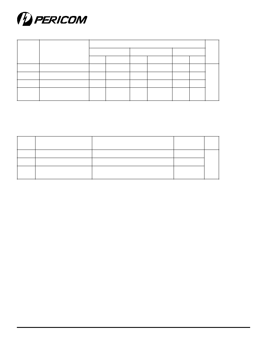
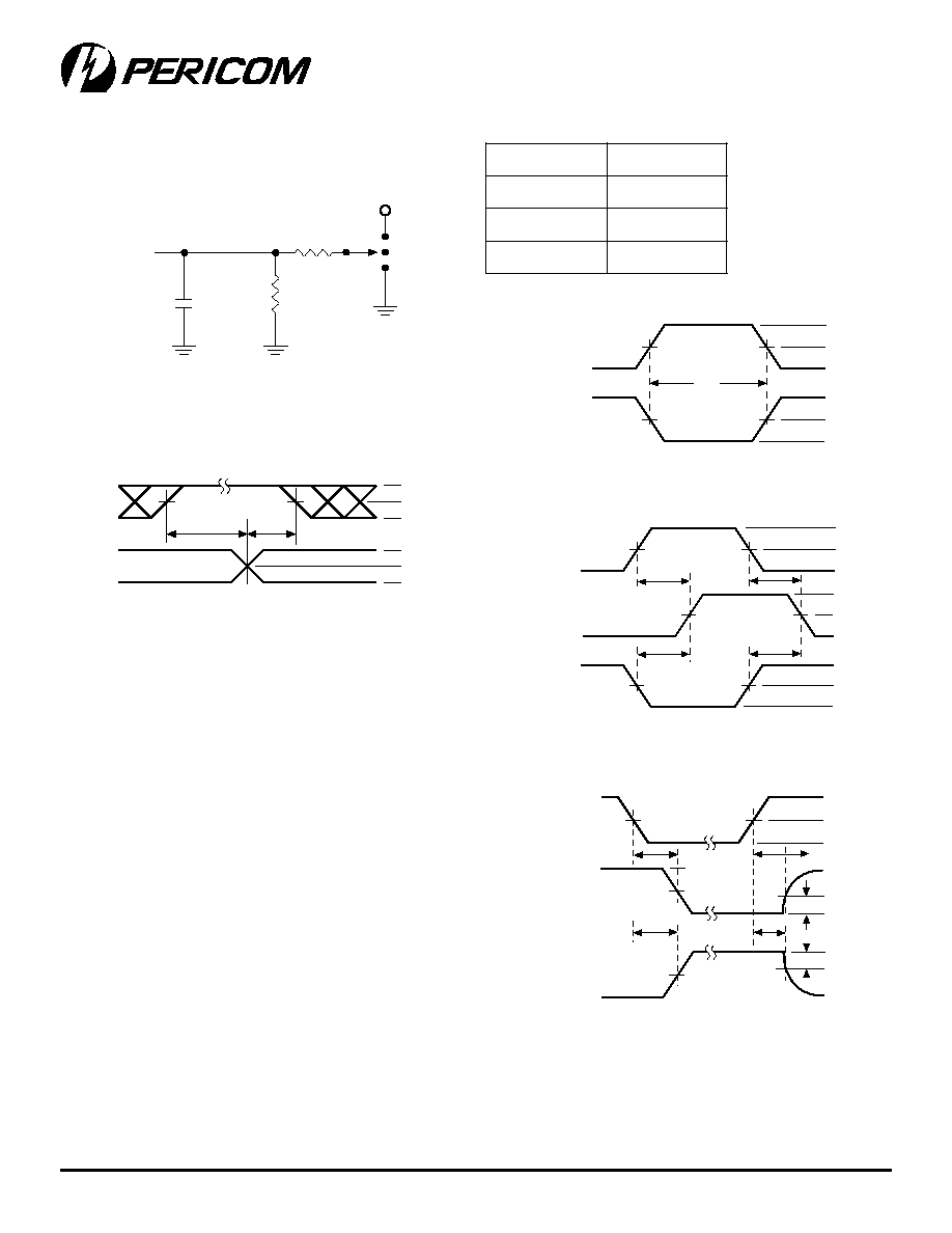
Test Circuits and Switching Waveforms
Parameter Measurement Information (V
DD
= 1.8V - 3.6V)
Setup, Hold, and Release Timing
Pulse Width
Switch Position
Propagation Delay
Enable Disable Timing
Data
Input
t
H
V
DD
t
SU
0V
Timing
Input
V
DD
0V
V
DD/2
V
DD/2
Low-High-Low
Pulse
t
W
High-Low-High
Pulse
V
DD
0V
V
DD
0V
V
DD/2
V
DD/2
Input
Opposite Phase
Input Transition
t
PLH
t
PHL
t
PLH
t
PHL
V
DD
0V
V
DD
V
OL
V
DD
0V
Output
V
DD/2
V
DD/2
V
DD/2
Notes:
A. C
L
includes probe and jig capacitance.
B. Waveform 1 is for an output with internal conditions
such that the output is LOW except when disabled by the
output control.
Waveform 2 is for an output with internal conditions
such that the output is HIGH except when disabled by
the output control.
C. All input pulses are supplied by generators having the
following characteristics: PRR
10 MHz, Z
O
= 50
,
t
r
2ns, t
f
2ns, measured from 10% to 90%, unless
otherwise specified.
D. The outputs are measured one at a time with one transi-
tion per measurement.
Pericom Semiconductor Corporation
2380 Bering Drive � San Jose, CA 95131 � 1-800-435-2336 � Fax (408) 435-1100 � http://www.pericom.com
Output
Control
(Active LOW)
Output
Waveform 2
S1 at GND
(see Note B)
t
PZL
t
PLZ
V
DD
0V
V
DD
V
OL
0V
Output
Waveform 1
S1 at 2xV
DD
(see Note B)
+0.15V
-0.15V
V
OH
V
DD
t
PHZ
t
PZH
V
DD/2
V
DD/2
V
DD
/2
C
L
R
1
500
50pF
From Output
Under Test
GND
2 x V
DD
Open
(See Note A)
R
L
500
t
s
e
T
1
S
t d
p
n
e
p
O
t
/
Z
L
P
T
L
Z
P
x
2 V
D
D
t
/
Z
H
P
T
H
Z
P
D
N
G