1
PS8354B 09/22/04
Description
Pericom Semiconductor's PI74ALVTC16245 is a 16-bit bidirectional
transceiver designed for asynchronous two-way communication
between data buses. The direction control input pin (xDIR)
determines the direction of data flow through the bidirectional
transceiver. The Direction and Output Enable controls are designed
to operate this device as either two independent 8-bit transceivers
or one 16-bit transceiver. The output enable (OE) input, when HIGH,
disables both A and B ports by placing them in Hi-Z condition.
To ensure the high-impedance state during power up or power
down, OE should be tied to Vdd through a pullup resistor; the
minimum value of the resistor is determined by the current-sinking
capability of the driver.
The family offers both I/O Tolerant, which allows it to operate in
mixed 1.8/3.6V systems, and "Bus Hold," which retains the data
input's last state whenever the data input goes to high-impedance,
preventing "floating" inputs and eliminating the need for pullup/
down resistors.
12345678901234567890123456789012123456789012345678901234567890121234567890123456789012345678901212345678901234567890123456789012123456789012
12345678901234567890123456789012123456789012345678901234567890121234567890123456789012345678901212345678901234567890123456789012123456789012
Features
∑ PI74ALVTC family is designed for low voltage operation,
V
DD
= 1.8V to 3.6V
∑ Supports Live Insertion
∑ 3.6V I/O Tolerant Inputs and Outputs
∑ Bus Hold
∑ High Drive, -32/64mA @ 3.3V
∑ Uses patented noise reduction circuitry
∑ Power-off high impedance inputs and outputs
∑ Industrial operation at ≠40∞C to +85∞C
∑ Packaging (Pb-free & Green available):
≠ 48-pin 240- mil wide plastic TSSOP (A)
≠ 48-pin 173-mil wide plastic TVSOP (K)
≠ 48-pin 300-mil wide plastic SSOP (V)
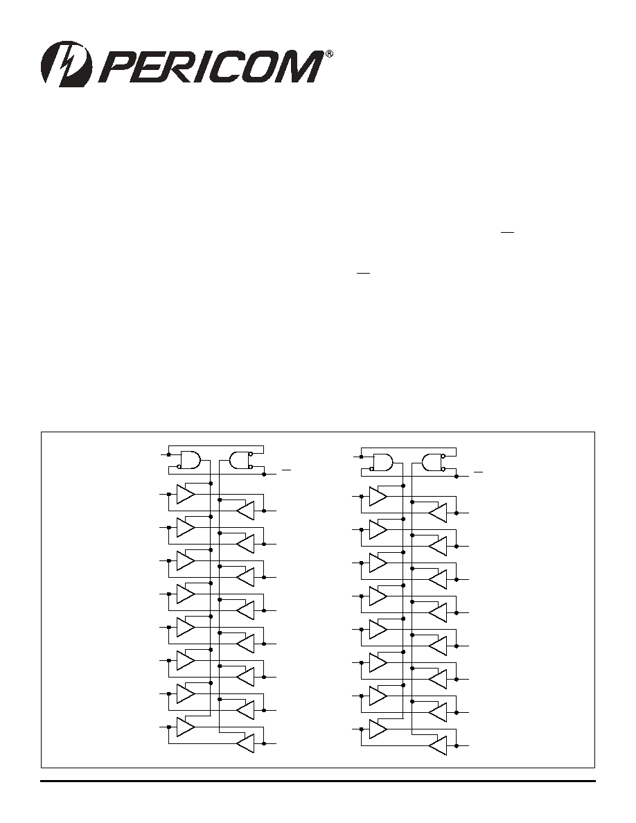
PI74ALVTC16245
16-Bit BiDirectional Transceiver
with 3-State Outputs
Block Diagram
1B
0
1A
0
1OE
1DIR
1B
1
1A
1
1B
2
1A
2
1B
3
1A
3
1B
4
1A
4
1B
5
1
A
5
1B
6
1A
6
1B
7
1A
7
2
B
0
2
A
0
2
OE
2
DIR
2
B
1
2
A
1
2
B
2
2
A
3
2
B
3
2
A
4
2
B
4
2
A
5
2
B
5
2
A
6
2
B
6
2
A
7
2
B
7
2
A
8
2
PS8354B 09/22/04
12345678901234567890123456789012123456789012345678901234567890121234567890123456789012345678901212345678901234567890123456789012123456789012
12345678901234567890123456789012123456789012345678901234567890121234567890123456789012345678901212345678901234567890123456789012123456789012
PI74ALVTC16245
16-Bit BiDirectional Transceiver
with 3-State Outputs
s
t
u
p
n
I
)
1
(
s
t
u
p
t
u
O
)
1
(
E
O
x
R
I
D
x
L
L
A
s
u
B
o
t
a
t
a
D
B
s
u
B
L
H
B
s
u
B
o
t
a
t
a
D
A
s
u
B
H
X
e
t
a
t
S
Z
h
g
i
H
e
m
a
N
n
i
P
n
o
i
t
p
i
r
c
s
e
D
O
x E
)
W
O
L
e
v
it
c
A
(
s
t
u
p
n
I
e
l
b
a
n
E
t
u
p
t
u
O
e
t
a
t
S
-
3
R
I
D
x
t
u
p
n
I
l
o
r
t
n
o
C
n
o
it
c
e
ri
D
X
A
X
s
t
u
p
n
I
e
t
a
t
S
-
3
r
o
s
t
u
p
n
I
A
e
d
i
S
X
B
X
s
t
u
p
t
u
O
e
t
a
t
S
-
3
r
o
s
t
u
p
n
I
B
e
d
i
S
D
N
G
d
n
u
o
r
G
V
CC
r
e
w
o
P
1
2
3
4
5
6
7
8
9
48
10
47
11
46
12
45
13
44
14
43
15
42
16
41
17
40
18
39
19
38
20
37
21
36
22
35
23
34
24
33
32
31
30
29
28
27
26
25
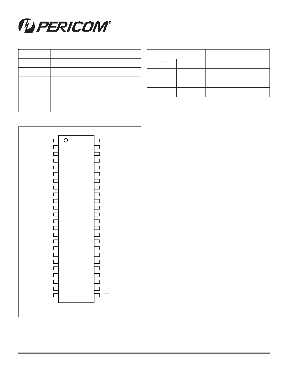
Product Pin Description
Truth Table
(1)
Notes:
1.
H = High Signal Level
L = Low Signal Level
X = Don't Care or Irrelevant
Z = High Impedance
Product Pin Configuration
48-Pin
A, K, V
1
OE
1
A
0
1
A
1
GND
1
A
2
1
A
3
V
CC
1
A
4
1
A
5
GND
1
A
6
1
A
7
2
A
0
2
A
1
GND
2
A
2
2
A
3
V
CC
2
A
4
2
A
5
GND
2
A
6
2
A
7
2
OE
1
DIR
1
B
0
1
B
1
GND
1
B
2
1
B
3
V
CC
1
B
4
1
B
5
GND
1
B
6
1
B
7
2
B
0
2
B
1
GND
2
B
2
2
B
3
V
CC
2
B
4
2
B
5
GND
2
B
6
2
B
7
2
DIR
3
PS8354B 09/22/04
12345678901234567890123456789012123456789012345678901234567890121234567890123456789012345678901212345678901234567890123456789012123456789012
12345678901234567890123456789012123456789012345678901234567890121234567890123456789012345678901212345678901234567890123456789012123456789012
PI74ALVTC16245
16-Bit BiDirectional Transceiver
with 3-State Outputs
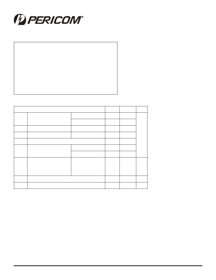
Stresses greater than those listed under MAXIMUM
RATINGS may cause permanent damage to the device.
This is a stress rating only and functional operation of the
device at these or any other conditions above those indi-
cated in the operational sections of this specification is not
implied. Exposure to absolute maximum rating conditions
for extended periods may affect reliability.
Supply Voltage Range, V
DD
.......................................... ≠0.5V to 4.6V
Input Voltage Range, V
I
................................................. -0.5V to 4.6V
Output Voltage Range, V
O
(3-Stated) ............................ -0.5V to 4.6V
Output Voltage Range, V
O
(1)
(Active) ................. ≠0.5V to V
DD
+0.5V
DC Input Diode Current (I
IK
) V
I
<0V ........................................ -50mA
DC Output Diode Current (I
OK
)
V
O
<0V ................................................................................... -50mA
V
O
>V
DD
................................................................................ +50mA
DC Output Source/Sink Current (I
OH
/I
OL
) ......................... -64/128mA
DC V
DD
or GND Current per Supply Pin (I
CC
or GND) ....... ±100mA
Storage Temperature Range, T
stg
...........................
≠65
∞
C to150
∞
C
Recommended Operating Conditions
2
Maximum Ratings
(Above which the useful life may be impaired. For user guidelines, not tested.)
Notes
1. Absolute maximum of I
O
must be observed.
2. Unused control inputs must be held HIGH or LOW to prevent them from floating.
3 As measured between 0.8V and 2.0V, V
DD
= 3.0V.
.
n
i
M
.
x
a
M
s
t
i
n
U
V
D
D
e
g
a
tl
o
v
y
l
p
p
u
S
g
n
it
a
r
e
p
O
8
.
1
6
.
3
V
y
l
n
O
n
o
it
n
e
t
e
R
a
t
a
D
2
.
1
6
.
3
V
H
I
e
g
a
tl
o
v
t
u
p
n
i
l
e
v
e
l
-
h
g
i
H
V
D
D
V
6
.
3
o
t
V
7
.
2
=
0
.
2
V
L
I
e
g
a
tl
o
v
t
u
p
n
i
l
e
v
e
l
-
w
o
L
V
D
D
V
6
.
3
o
t
V
7
.
2
=
8
.
0
V
I
e
g
a
tl
o
v
t
u
p
n
I
3
.
0
-
6
.
3
V
O
e
g
a
tl
o
v
t
u
p
t
u
O
e
t
a
t
S
e
v
it
c
A
0
V
D
D
e
t
a
t
S
f
f
O
0
6
.
3
I
O
I
n
i
t
n
e
r
r
u
c
t
u
p
t
u
O
H
O
I
/
L
O
V
D
D
V
6
.
3
o
t
V
0
.
3
=
V
D
D
V
0
.
3
o
t
V
7
.
2
=
V
D
D
V
7
.
2
o
t
V
3
.
2
=
V
D
D
V
8
.
1
=
4
6
/
2
3
-
4
2
±
8
1
±
6
±
A
m
/t
v
e
t
a
r
ll
a
f
r
o
e
s
i
r
n
o
it
s
i
s
n
a
r
t
t
u
p
n
I
)
3
(
0
0
1
V
/
s
n
T
A
e
r
u
t
r
e
p
m
e
t
ri
a
-
e
e
r
f
g
n
it
a
r
e
p
O
0
4
-
5
8
C
4
PS8354B 09/22/04
12345678901234567890123456789012123456789012345678901234567890121234567890123456789012345678901212345678901234567890123456789012123456789012
12345678901234567890123456789012123456789012345678901234567890121234567890123456789012345678901212345678901234567890123456789012123456789012
PI74ALVTC16245
16-Bit BiDirectional Transceiver
with 3-State Outputs
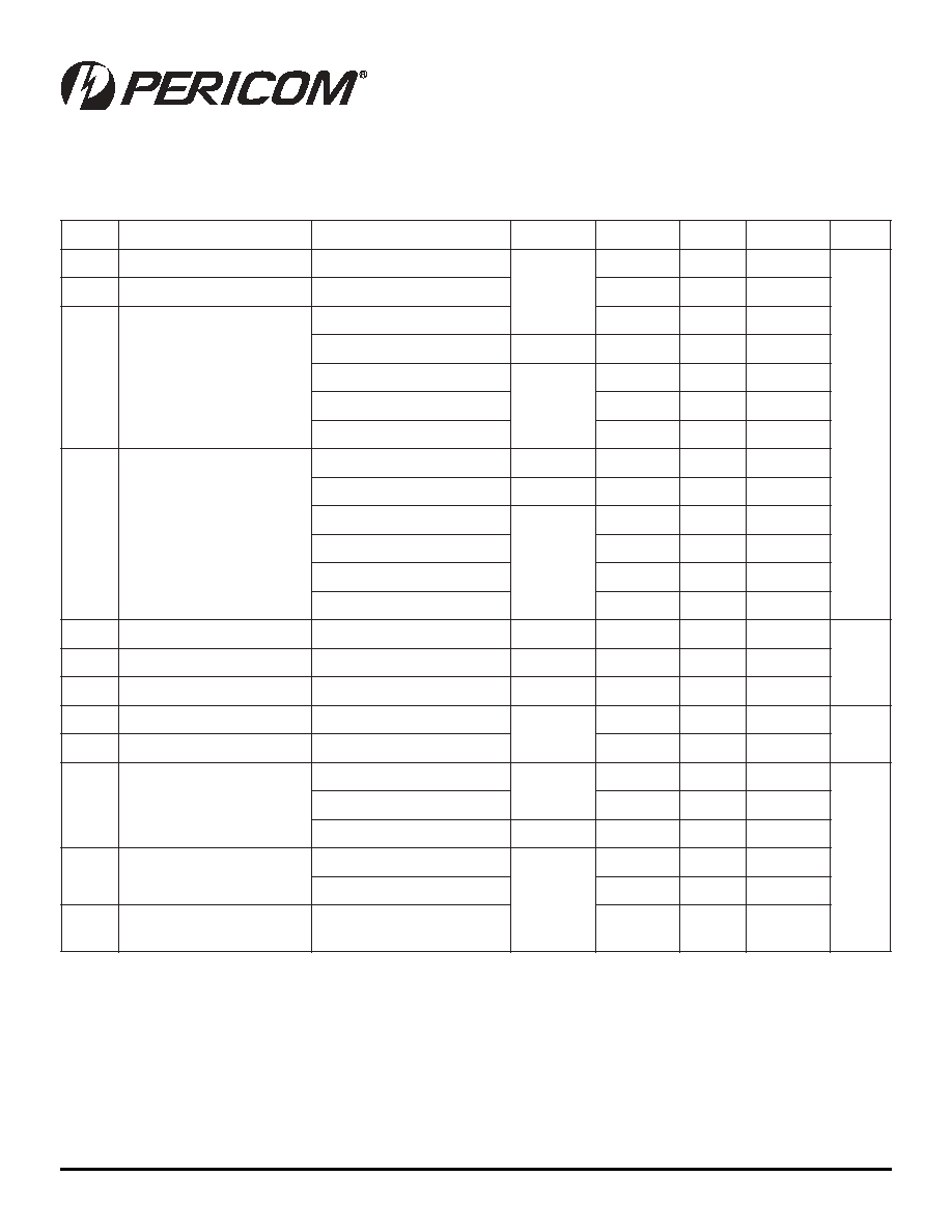
Electrical Characteristics over Recommended Operating Free-Air Temperature Range
(unless otherwise noted)
DC Characteristics (2.7V<V
DD
3.6V)
Notes
1. Duration of test must not exceed 1 second with only 1 output tested at a time.
r
e
t
e
m
a
r
a
P
s
n
o
i
t
i
d
n
o
C
V
D
D
.
n
i
M
.
p
y
T
.
x
a
M
s
t
i
n
U
V
H
I
e
g
a
tl
o
V
t
u
p
n
I
l
e
v
e
L
H
G
I
H
6
.
3
-
7
.
2
0
.
2
V
V
L
I
e
g
a
tl
o
V
t
u
p
n
I
l
e
v
e
L
W
O
L
8
.
0
V
H
O
e
g
a
tl
o
V
t
u
p
t
u
O
l
e
v
e
L
H
G
I
H
I
H
O
=
-
0
0
1
µ
A
V
D
D
2
.
0
-
I
H
O
=
-
A
m
2
1
7
.
2
2
.
2
I
H
O
=
-
A
m
8
1
0
.
3
4
.
2
I
H
O
=
-
A
m
4
2
2
.
2
I
H
O
=
-
A
m
2
3
0
.
2
V
L
O
e
g
a
tl
o
V
t
u
p
t
u
O
l
e
v
e
L
W
O
L
I
L
O
=
0
0
1
µ
A
6
.
3
-
7
.
2
2
.
0
I
L
O
= 2
1
A
m
7
.
2
4
.
0
I
L
O
= 8
1
A
m
0
.
3
4
.
0
I
L
O
= 4
2
A
m
5
4
.
0
I
L
O
= 2
3
A
m
5
.
0
I
L
O
= 4
6
A
m
5
5
.
0
I
I
t
n
e
r
r
u
C
e
g
a
k
a
e
L
t
u
p
n
I
V
I
V
=
D
D
D
N
G
r
o
,
6
.
3
0
.
5
±
µ
A
I
Z
O
e
g
a
k
a
e
L
t
u
p
t
u
O
E
T
A
T
S
-
3
V
O
V
6
.
3
=
7
.
2
0
1
±
I
F
F
O
t
n
e
r
r
u
C
e
g
a
k
a
e
L
F
F
O
-
r
e
w
o
P
V
I
V
r
o
O
V
6
.
3
0
0
1
I
L
D
O
w
o
L
t
n
e
r
r
u
C
t
u
p
t
u
O
V
IN
=
V
IH
V
r
o
IL
,
V
5
.
1
=
o
V
)
1
(
6
.
3
0
5
1
4
3
3
A
m
I
H
D
O
h
g
i
H
t
n
e
r
r
u
C
t
u
p
t
u
O
V
IN
=
V
IH
V
r
o
IL
,
V
5
.
1
=
o
V
)
1
(
8
5
-
4
1
1
-
I
D
L
O
H
t
n
e
r
r
u
C
d
l
o
H
s
u
B
s
t
u
p
t
u
O
B
r
o
A
V
I
V
8
.
0
=
0
.
3
5
7
µ
A
V
I
V
0
.
2
=
5
7
-
V
I
V
6
.
3
o
t
0
=
6
.
3
0
0
5
±
I
D
D
t
n
e
r
r
u
C
y
l
p
p
u
S
t
n
e
c
s
e
i
u
Q
V
I
V
=
D
D
D
N
G
r
o
6
.
3
-
7
.
2
0
5
V
D
D
V
(
I
V
,
O
)
V
6
.
3
0
5
±
I
D
D
I
n
i
e
s
a
e
r
c
n
I
D
D
t
u
p
n
i
r
e
p
V
H
I
V
=
D
D
,
V
6
.
0
-
V
t
a
s
t
u
p
n
i
r
e
h
t
O
D
D
d
n
G
r
o
0
0
4

5
PS8354B 09/22/04
12345678901234567890123456789012123456789012345678901234567890121234567890123456789012345678901212345678901234567890123456789012123456789012
12345678901234567890123456789012123456789012345678901234567890121234567890123456789012345678901212345678901234567890123456789012123456789012
PI74ALVTC16245
16-Bit BiDirectional Transceiver
with 3-State Outputs
DC Characteristics (2.3V
V
DD
2.7V)
Notes:
1. Not Guaranteed
2. Duration of test must not exceed 1 second with only 1 output tested at a time.
n
o
i
t
p
i
r
c
s
e
D
s
r
e
t
e
m
a
r
a
P
s
n
o
i
t
i
d
n
o
C
V
D
D
.
n
i
M
.
p
y
T
.
x
a
M
s
t
i
n
U
V
H
I
e
g
a
tl
o
V
t
u
p
n
I
l
e
v
e
L
H
G
I
H
7
.
2
-
3
.
2
6
.
1
V
V
L
I
e
g
a
tl
o
V
t
u
p
n
I
l
e
v
e
L
W
O
L
7
.
0
V
H
O
e
g
a
tl
o
V
t
u
p
t
u
O
l
e
v
e
L
H
G
I
H
I
H
O
0
0
1
-
=
µ
A
V
D
D
2
.
0
-
I
H
O
A
m
2
1
-
=
3
.
2
8
.
1
I
H
O
A
m
8
1
-
=
7
.
1
V
L
O
e
g
a
tl
o
V
t
u
p
t
u
O
l
e
v
e
L
W
O
L
I
L
O
0
0
1
=
µ
A
7
.
2
-
3
.
2
2
.
0
I
L
O
A
m
2
1
=
3
.
2
4
.
0
I
L
O
A
m
8
1
=
5
.
0
I
L
O
A
m
4
2
=
5
5
.
0
I
I
t
n
e
r
r
u
C
e
g
a
k
a
e
L
t
u
p
n
I
V
1
V
=
D
D
D
N
G
r
o
7
.
2
0
.
5
±
µ
A
I
Z
O
e
g
a
k
a
e
L
t
u
p
t
u
O
E
T
A
T
S
-
3
V
O
6
.
3
=
V
3
.
2
0
1
±
I
F
F
O
t
n
e
r
r
u
C
e
g
a
k
a
e
L
F
F
O
-
r
e
w
o
P
V
I
V
r
o
O
6
.
3
V
0
0
1
I
L
D
O
w
o
L
t
n
e
r
r
u
C
t
u
p
t
u
O
V
N
I
=
V
H
I
r
o V
,
L
I
V
O
=
V
5
.
1
)
2
(
7
.
2
0
1
1
4
6
2
A
m
I
H
D
O
h
g
i
H
t
n
e
r
r
u
C
t
u
p
t
u
O
V
N
I
=
V
H
I
r
o V
,
L
I
V
O
=
V
5
.
1
)
2
(
0
3
-
0
6
-
I
D
L
O
H
)
1
(
t
n
e
r
r
u
C
d
l
o
H
s
u
B
s
t
u
p
t
u
O
B
r
o
A
V
I
V
7
.
0
=
5
.
2
0
9
µ
A
V
I
V
7
.
1
=
0
9
-
I
D
D
t
n
e
r
r
u
C
y
l
p
p
u
S
t
n
e
c
s
e
i
u
Q
V
I
V
=
D
D
D
N
G
r
o
7
.
2
-
3
.
2
0
4
V
D
D
V
(
I
V
,
O
)
V
6
.
3
0
4
±
D
D
n
i
e
s
a
e
r
c
n
I
I
D
D
t
u
p
n
i
r
e
p
V
H
I
V
=
D
D
,
V
6
.
0
-
V
t
a
s
t
u
p
n
I
D
D
d
n
G
r
o
0
0
4
Electrical Characteristics over Recommended Operating Free-Air Temperature Range
(unless otherwise noted)