1
PS8619 06/05/02
Product Description
Pericom Semiconductors PI74ALVTC series of logic circuits are
produced using the Companys advanced 0.35 micron CMOS
technology, achieving industry leading speed.
12345678901234567890123456789012123456789012345678901234567890121234567890123456789012345678901212345678901234567890123456789012123456789012
12345678901234567890123456789012123456789012345678901234567890121234567890123456789012345678901212345678901234567890123456789012123456789012
PI74ALVTC16827
2.5V 20-Bit Buffer/Driver
with 3-State Outputs
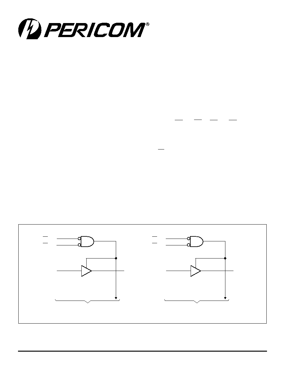
Logic Block Diagram
Product Features
PI74ALVTC16827 is designed for low voltage operation,
V
DD
= 1.65V to 3.6V
Supports Live Insertion
3.6V I/O Tolerant Inputs and Outputs
Bus Hold
High Drive, 32/64mA @ 3.3V
Uses patented noise reduction circuitry
Power-off high impedance inputs and outputs
Industrial operation at 40∞C to +85∞C
Packages available:
56-pin 240-mil wide plastic TSSOP (A56)
56-pin 173-mil wide plastic TVSOP (K56)
1OE
1
1OE
2
1Y1
1
2
55
56
1A1
To 9 Other Channels
2OE
1
2OE
2
2Y1
28
15
42
29
2A1
To 9 Other Channels
The PI74ALVTC16827, is a 20-Bit non-inverting buffer/driver
designed for 1.65V to 3.6V Vcc operation.
A buffer/driver is composed of two 10-bit sections with separate
output-enable signals. For either 10-Bit buffer section, the two
output-enable (1OE1 and 1OE2 or 2OE1 and 2OE2 inputs must both
be low for the corresponding Y outputs to be active. If either output-
enable input is HIGH, the output of that 10-Bit buffer section are in
the high-impedance state.
To ensure the high-impedance state during power up or power
down, OE should be tied to Vcc through a pullup resistor whose
minimum value is determined by the current sinking capability of
the driver.
The family offers both I/O Tolerant, which allows it to operate in
mixed 1.65/3.6V systems, and Bus Hold, which retains the data
inputs last state preventing floating inputs and eliminating the
need for pullup/down resistors.
2
PS8619 06/05/02
12345678901234567890123456789012123456789012345678901234567890121234567890123456789012345678901212345678901234567890123456789012123456789012
12345678901234567890123456789012123456789012345678901234567890121234567890123456789012345678901212345678901234567890123456789012123456789012
PI74ALVTC16827
2.5V 20-Bit Buffer /Driver
with 3-State Outputs
1
2
3
4
5
6
7
8
9
10
11
12
13
14
15
16
17
18
19
20
21
22
23
24
56
55
54
53
52
51
50
49
48
47
46
45
44
43
42
41
40
39
38
37
36
35
34
33
25
26
27
28
32
31
30
29
1OE1
1Y1
1Y2
GND
1Y3
1Y4
VCC
1Y5
1Y6
1Y7
GND
1Y8
1Y9
1Y10
2Y1
2Y2
2Y3
GND
2Y4
2Y5
2Y6
VCC
2Y7
2Y8
GND
2Y9
2Y10
2OE1
1OE2
1A1
1A2
GND
1A3
1A4
VCC
1A5
1A6
1A7
GND
1A8
1A9
1A10
2A1
2A2
2A3
GND
2A4
2A5
2A6
VCC
2A7
2A8
GND
2A9
2A10
2OE2
e
m
a
N
n
i
P
n
o
it
p
i
r
c
s
e
D
OE
)
W
O
L
e
v
it
c
A
(
st
u
p
n
I
el
b
a
n
E
t
u
p
t
u
O
A
X
st
u
p
n
I
a
t
a
D
Y
X
st
u
p
t
u
O
e
t
a
t
S
-
3
D
N
G
d
n
u
o
r
G
V
CC
r
e
w
o
P
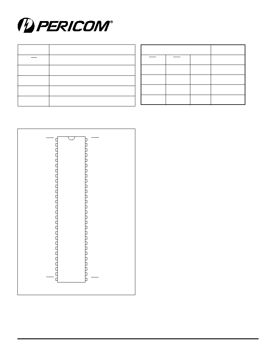
Product Pin Description
Truth Table
(1)
Note:
1. H = High Signal Level
L = Low Signal Level
X = Irrelevant
Z = High Impedance
Product Pin Configuration
s
t
u
p
n
I
s
t
u
p
t
u
O
1
E
O
2
E
O
A
Y
L
L
L
L
L
L
H
H
H
X
X
Z
X
H
X
Z
56-pin
A, K

3
PS8619 06/05/02
12345678901234567890123456789012123456789012345678901234567890121234567890123456789012345678901212345678901234567890123456789012123456789012
12345678901234567890123456789012123456789012345678901234567890121234567890123456789012345678901212345678901234567890123456789012123456789012
PI74ALVTC16827
2.5V 20-Bit Buffer /Driver
with 3-State Outputs
Note:
Stresses greater than those listed under MAXIMUM
RATINGS may cause permanent damage to the device. This
is a stress rating only and functional operation of the device
at these or any other conditions above those indicated in the
operational sections of this specification is not implied.
Exposure to absolute maximum rating conditions for
extended periods may affect reliability.
Supply Voltage Range, V
DD ........................................................
0.5V to 4.6V
Input Voltage Range, V
I .................................................................
-0.5V to 4.6V
Output Voltage Range, V
O
(3-Stated) ............................... -0.5V to 4.6V
Output Voltage Range, V
O(1)
(Active) .................. 0.5V to V
DD
+0.5V
DC Input Diode Current (I
IK
) V
I
< 0V ........................................ 50mA
DC Output Diode Current (I
OK
)
V
O
< 0V.................................................................................... -50mA
V
O
> V
DD ....................................................................................................
±50mA
DC Output Source/Sink Current (I
OH
/I
OL
) .......................... -64/128mA
DC V
DD
or GND Current per Supply Pin (I
CC
or GND)............ ±100mA
Storage Temperature Range, T
stg
.................................. 65∞C to150∞C
Recommended Operating Conditions
(2)
Maximum Ratings
(Above which the useful life may be impaired. For user guidelines, not tested.)
Notes:
1. Absolute maximum of I
O
must be observed.
2. Unused control inputs must be held HIGH or LOW to prevent them from floating.
3 As measured between 0.8V and 2.0V, V
DD
= 3.0V.
.
n
i
M
.
x
a
M
s
ti
n
U
V
D
D
e
g
a
tl
o
v
y
l
p
p
u
S
g
n
it
a
r
e
p
O
5
6
.
1
6
.
3
V
y
l
n
O
n
o
it
n
e
t
e
R
a
t
a
D
2
.
1
6
.
3
V
H
I
e
g
a
tl
o
v
t
u
p
n
i
l
e
v
el
-
h
g
i
H
V
D
D
V
6
.
3
o
t
V
7
.
2
=
0
.
2
V
L
I
e
g
a
tl
o
v
t
u
p
n
i
l
e
v
el
-
w
o
L
V
D
D
V
6
.
3
o
t
V
7
.
2
=
8
.
0
V
I
e
g
a
tl
o
v
t
u
p
n
I
3
.
0
6
.
3
V
O
e
g
a
tl
o
v
t
u
p
t
u
O
e
t
a
t
S
e
v
it
c
A
0
V
D
D
e
t
a
t
S
ff
O
0
6
.
3
I
n
i
t
n
e
rr
u
c
t
u
p
t
u
O
H
O
I/
L
O
V
D
D
V
6
.
3
o
t
V
0
.
3
=
V
D
D
V
6
.
3
o
t
V
0
.
3
=
V
D
D
V
7
.
2
o
t
V
3
.
2
=
V
D
D
V
5
9
.
1
o
t
V
5
6
.
1
=
4
6
/
2
3
4
2
±
8
1
±
6
±
A
m
/t
v
e
t
a
r
ll
a
f
r
o
e
si
r
n
o
it
si
s
n
a
rt
t
u
p
n
I
)
3
(
0
0
1
V
/
s
n
T
A
e
r
u
t
a
r
e
p
m
e
t
ri
a
-
e
e
rf
g
n
it
a
r
e
p
O
-
0
4
5
8
C

4
PS8619 06/05/02
12345678901234567890123456789012123456789012345678901234567890121234567890123456789012345678901212345678901234567890123456789012123456789012
12345678901234567890123456789012123456789012345678901234567890121234567890123456789012345678901212345678901234567890123456789012123456789012
PI74ALVTC16827
2.5V 20-Bit Buffer /Driver
with 3-State Outputs
Electrical Characteristics over Recommended Operating Free-Air Temperature Range
(unless otherwise noted)
DC Characteristics (2.7V<V
DD
3.6V)
r
e
t
e
m
a
r
a
P
s
n
o
it
i
d
n
o
C
V
D
D
.
n
i
M
.
p
y
T
.
x
a
M
s
ti
n
U
V
K
I
e
d
o
i
D
p
m
al
C
t
u
p
n
I
I
K
I
=
-
A
m
8
1
0
.
3
2
.
1
V
V
H
O
e
g
a
tl
o
V
t
u
p
t
u
O
l
e
v
e
L
H
G
I
H
I
H
O
=
-
0
0
1
µ
A
6
.
3
-
7
.
2
V
D
D
2
.
0
I
H
O
=
-
A
m
2
1
7
.
2
2
.
2
I
H
O
=
-
A
m
8
1
0
.
3
4
.
2
I
H
O
=
-
A
m
4
2
2
.
2
I
H
O
=
-
A
m
2
3
0
.
2
V
L
O
e
g
a
tl
o
V
t
u
p
t
u
O
l
e
v
e
L
W
O
L
I
L
O
=
0
0
1
µ
A
6
.
3
-
7
.
2
2
.
0
I
L
O
= 2
1 A
m
7
.
2
4
.
0
I
L
O
= 8
1 A
m
0
.
3
4
.
0
I
L
O
= 4
2 A
m
5
4
.
0
I
L
O
= 2
3 A
m
5
.
0
I
L
O
= 4
6 A
m
5
5
.
0
I
I
t
n
e
rr
u
C
e
g
a
k
a
e
L
t
u
p
n
I
V
I
V
=
D
D
D
N
G
r
o
,
6
.
3
0
.
5
±
µ
A
I
Z
O
e
g
a
k
a
e
L
t
u
p
t
u
O
e
t
a
t
S
-
3
V
O
V
6
.
3
=
7
.
2
0
1
±
I
F
F
O
t
n
e
rr
u
C
e
g
a
k
a
e
L
F
F
O
-r
e
w
o
P
V
I
V
r
o
O
V
6
.
3
0
0
1
I
D
L
O
H
t
n
e
rr
u
C
d
l
o
H
s
u
B
st
u
p
t
u
O
B
r
o
A
V
I
V
8
.
0
=
0
.
3
5
7
V
I
V
0
.
2
=
5
7
V
I
V
6
.
3
o
t
0
=
6
.
3
0
0
5
±
I
D
D
t
n
e
rr
u
C
y
l
p
p
u
S
t
n
e
c
s
ei
u
Q
V
I
V
=
D
D
D
N
G
r
o
6
.
3
-
7
.
2
0
5
V
D
D
V
(
I
V
,
O
)
V
6
.
3
0
5
±
I
D
D
I
n
i
e
s
a
e
r
c
n
I
D
D
t
u
p
n
i
r
e
p
V
H
I
V
=
D
D
,
V
6
.
0
V
t
a
st
u
p
n
i
r
e
h
t
O
D
D
d
n
G
r
o
0
0
4

5
PS8619 06/05/02
12345678901234567890123456789012123456789012345678901234567890121234567890123456789012345678901212345678901234567890123456789012123456789012
12345678901234567890123456789012123456789012345678901234567890121234567890123456789012345678901212345678901234567890123456789012123456789012
PI74ALVTC16827
2.5V 20-Bit Buffer /Driver
with 3-State Outputs
DC Characteristics (2.3V
V
DD
2.7V)
Note:
1. Not Guaranteed
n
o
it
p
i
r
c
s
e
D
s
r
e
t
e
m
a
r
a
P
s
n
o
it
i
d
n
o
C
V
D
D
.
n
i
M
.
p
y
T
.
x
a
M
s
ti
n
U
V
K
I
e
d
o
i
D
p
m
al
C
t
u
p
n
I
I
K
I
A
m
8
1
=
3
.
2
2
.
1
V
V
H
O
e
g
a
tl
o
V
t
u
p
t
u
O
l
e
v
e
L
H
G
I
H
I
H
O
0
0
1
=
µ
A
7
.
2
-
3
.
2
V
D
D
2
.
0
I
H
O
A
m
2
1
=
3
.
2
8
.
1
I
H
O
A
m
8
1
=
7
.
1
V
L
O
e
g
a
tl
o
V
t
u
p
t
u
O
l
e
v
e
L
W
O
L
I
L
O
0
0
1
=
µ
A
7
.
2
-
3
.
2
2
.
0
I
L
O
A
m
2
1
=
3
.
2
4
.
0
I
L
O
A
m
8
1
=
5
.
0
I
L
O
A
m
4
2
=
5
5
.
0
I
I
t
n
e
rr
u
C
e
g
a
k
a
e
L
t
u
p
n
I
V
I
V
=
D
D
D
N
G
r
o
7
.
2
0
.
5
±
µ
A
I
Z
O
e
g
a
k
a
e
L
t
u
p
t
u
O
e
t
a
t
S
-
3
V
O
6
.
3
=
V
3
.
2
0
1
±
I
F
F
O
t
n
e
rr
u
C
e
g
a
k
a
e
L
F
F
O
-r
e
w
o
P
V
I
V
r
o
O
6
.
3
V
0
0
1
I
D
L
O
H
)
1
(
t
n
e
rr
u
C
d
l
o
H
s
u
B
st
u
p
t
u
O
B
r
o
A
V
I
V
7
.
0
=
5
.
2
0
9
µ
A
V
I
V
7
.
1
=
0
9
I
D
D
t
n
e
rr
u
C
y
l
p
p
u
S
t
n
e
c
s
ei
u
Q
V
I
V
=
D
D
D
N
G
r
o
7
.
2
-
3
.
2
0
4
V
D
D
V
(
I
V
,
O
)
V
6
.
3
0
4
±
D
D
n
i
e
s
a
e
r
c
n
I
I
D
D
t
u
p
n
i
r
e
p
V
H
I
V
=
D
D
,
V
6
.
0
V
t
a
st
u
p
n
I
D
D
d
n
G
r
o
0
0
4
Electrical Characteristics over Recommended Operating Free-Air Temperature Range
(unless otherwise noted; continued from previous page)

6
PS8619 06/05/02
12345678901234567890123456789012123456789012345678901234567890121234567890123456789012345678901212345678901234567890123456789012123456789012
12345678901234567890123456789012123456789012345678901234567890121234567890123456789012345678901212345678901234567890123456789012123456789012
PI74ALVTC16827
2.5V 20-Bit Buffer /Driver
with 3-State Outputs
DC Characteristics (1.65V
V
DD
1.95V)
Electrical Characteristics over Recommended Operating Free-Air Temperature Range
(unless otherwise noted; continued from previous page)
Note:
1. Not Guaranteed
n
o
it
p
i
r
c
s
e
D
s
r
e
t
e
m
a
r
a
P
s
n
o
it
i
d
n
o
C
V
D
D
.
n
i
M
.
p
y
T
.
x
a
M
s
ti
n
U
V
K
I
e
d
o
i
D
p
m
al
C
t
u
p
n
I
I
K
I
A
m
8
1
=
5
6
.
1
2
.
1
V
V
H
O
e
g
a
tl
o
V
t
u
p
t
u
O
l
e
v
e
L
H
G
I
H
I
H
O
0
0
1
=
µ
A
5
9
.
1
-
5
6
.
1
V
D
D
2
.
0
I
H
O
A
m
6
=
5
6
.
1
4
.
1
V
L
O
e
g
a
tl
o
V
t
u
p
t
u
O
l
e
v
e
L
W
O
L
I
L
O
0
0
1
=
µ
A
2
.
0
I
L
O
A
m
6
=
3
.
0
I
I
t
n
e
rr
u
C
e
g
a
k
a
e
L
t
u
p
n
I
V
I
V
=
D
D
D
N
G
r
o
5
9
.
1
0
.
5
±
µ
A
I
Z
O
e
g
a
k
a
e
L
t
u
p
t
u
O
e
t
a
t
S
-
3
V
O
6
.
3
=
V
5
6
.
1
0
1
±
I
F
F
O
t
n
e
rr
u
C
e
g
a
k
a
e
L
F
F
O
-r
e
w
o
P
V
I
V
=
O
6
.
3
V
0
0
1
I
D
L
O
H
)
1
(
t
n
e
rr
u
C
d
l
o
H
s
u
B
st
u
p
t
u
O
B
r
o
A
V
I
4
.
0
=
5
6
.
1
0
5
V
I
3
.
1
=
0
5
I
D
D
t
n
e
rr
u
C
y
l
p
p
u
S
t
n
e
c
s
ei
u
Q
V
I
V
=
D
D
D
N
G
r
o
5
9
.
1
-
5
6
.
1
0
2
V
D
D
V
(
I
V
,
O
)
V
6
.
3
0
2
±
D
D
n
i
e
s
a
e
r
c
n
I
I
D
D
t
u
p
n
i
r
e
p
V
I
V
=
D
D
,
V
6
0
V
t
a
st
u
p
n
i
r
e
h
t
O
D
D
d
n
G
r
o
0
0
4
s
r
e
t
e
m
a
r
a
P
m
o
r
F
)t
u
p
n
I
(
o
T
)t
u
p
t
u
O
(
V
C
C
V
5
1
.
0
±
V
8
.
1
=
V
C
C
V
2
.
0
±
V
5
.
2
=
V
C
C
V
3
.
0
±
V
3
.
3
=
s
ti
n
U
.
n
i
M
.
x
a
M
.
n
i
M
.
x
a
M
.
n
i
M
.
x
a
M
t
d
p
A
Y
0
.
4
0
.
1
5
.
3
0
.
1
0
.
3
s
n
t
n
e
E
O
Y
5
.
5
6
.
1
0
.
5
6
.
1
0
.
4
t
si
d
E
O
Y
5
.
5
2
.
2
0
.
5
2
.
2
0
.
4
Switching Characteristics over recommended operating free-air temperature range
(unless otherwise noted, see Figures 1 thru 4)
7
PS8619 06/05/02
12345678901234567890123456789012123456789012345678901234567890121234567890123456789012345678901212345678901234567890123456789012123456789012
12345678901234567890123456789012123456789012345678901234567890121234567890123456789012345678901212345678901234567890123456789012123456789012
PI74ALVTC16827
2.5V 20-Bit Buffer /Driver
with 3-State Outputs
Test Circuits and Switching Waveforms
Parameter Measurement Information (V
DD
= 1.65V - 3.6V)
Setup, Hold, and Release Timing
Pulse Width
Switch Position
Propagation Delay
Enable Disable Timing
Notes:
A. C
L
includes probe and jig capacitance.
B. Waveform 1 is for an output with internal conditions
such that the output is LOW except when disabled by
the output control.
Waveform 2 is for an output with internal conditions
such that the output is HIGH except when disabled by
the output control.
C. All input pulses are supplied by generators having the
following characteristics: PRR
10 MHz, Z
O
= 50
,
t
r
2ns, t
f
2ns, measured from 10% to 90%, unless
otherwise specified.
D. The outputs are measured one at a time with one
transition per measurement.
C
L
R
1
500
30pF
From Output
Under Test
3.3V/2.5V V
DD
GND
2 x V
DD
Open
(See Note A)
R
L
500
C
L
R
1
1k
30pF
From Output
Under Test
1.8V V
DD
GND
2 x V
DD
Open
(See Note A)
R
L
1k
Data
Input
t
H
V
DD
t
SU
0V
Timing
Input
V
DD
0V
V
DD/2
V
DD/2
t
s
e
T
1
S
t
D
P
n
e
p
O
t
Z
L
P
/t
L
Z
P
x
2 V
D
D
t
Z
H
P
/t
H
Z
P
D
N
G
Low-High-Low
Pulse
t
W
High-Low-High
Pulse
V
DD
0V
V
DD
0V
V
DD/2
V
DD/2
Input
t
PLH
t
PLH
t
PHL
0V
0V
Output
Opposite Phase
Input Transition
V
DD
V
OL
t
PHL
V
DD/2
V
DD/2
V
DD/2
V
DD
V
DD
Output
Control
(Active LOW)
Output
Waveform 2
S1 at GND
(see Note B)
t
PZL
t
PLZ
V
DD
0V
V
DD
V
OL
0V
Output
Waveform 1
S1 at 2xV
DD
(see Note B)
+0.15V
-0.15V
V
OH
V
DD
t
PHZ
t
PZH
V
DD/2
V
DD/2
V
DD
/2

8
PS8619 06/05/02
12345678901234567890123456789012123456789012345678901234567890121234567890123456789012345678901212345678901234567890123456789012123456789012
12345678901234567890123456789012123456789012345678901234567890121234567890123456789012345678901212345678901234567890123456789012123456789012
PI74ALVTC16827
2.5V 20-Bit Buffer /Driver
with 3-State Outputs
56-Pin TSSOP Package (A)
56-Pin TVSOP Package (K)
Ordering Information
e
d
o
C
g
n
i
r
e
d
r
O
e
p
y
T
e
g
a
k
c
a
P
e
g
n
a
R
g
n
i
r
e
d
r
O
A
7
2
8
6
1
C
T
V
L
A
4
7
I
P
P
O
S
S
T
li
m
-
0
4
2
n
i
P
-
6
5
C
∞
5
8
o
t
C
∞
0
4
K
7
2
8
6
1
C
T
V
L
A
4
7
I
P
P
O
S
V
T
li
m
-
3
7
1
n
i
P
-
6
5
.002
.006
SEATING PLANE
.007
.011
.004
.008
1
56
.236
.244
0.50
0.17
0.27
0.05
0.15
0.09
0.20
X.XX
X.XX
DENOTES DIMENSIONS
IN MILLIMETERS
.018
.030
0.45
0.75
.047
Max.
1.20
6.0
6.2
.547
.555
13.9
14.1
.319
8.1
.0197
BSC
BSC
.047
.031
.041
SEATING
PLANE
.016
BSC
1
56
.169
.177
11.20
11.40
4.30
4.50
1.20
0.40
0.13
0.23
0.80
1.05
X.XX
X.XX
DENOTES DIMENSIONS
IN MILLIMETERS
.002
.006
0.05
0.15
.0035
.008
0.09
0.20
.018
.030
0.45
0.75
6.4
.252
BSC
.005
.009
.441
.449
Max.
Pericom Semiconductor Corporation
2380 Bering Drive ∑ San Jose, CA 95131 ∑ 1-800-435-2336 ∑ Fax (408) 435-1100 ∑ http://www.pericom.com