PI74FCT162245MT
16-BIT BIDIRECTIONAL TRANSCEIVERS
1
PS2046A 03/12/96
12345678901234567890123456789012123456789012345678901234567890121234567890123456789012345678901212345678901234567890123456789012123456789012
12345678901234567890123456789012123456789012345678901234567890121234567890123456789012345678901212345678901234567890123456789012123456789012
12345678901234567890123456789012123456789012345678901234567890121234567890123456789012345678901212345678901234567890123456789012123456789012
PI74FCT162245MT
Fast CMOS 16-Bit
Heavy Load
Bidirectional Transceivers
Product Description:
Pericom Semiconductor's PI74FCT series of logic circuits are pro-
duced in the Company's advanced 0.6 micron CMOS technology,
achieving industry leading speed grades.
The PI74FCT162245MT is a 16-bit bidirectional transceivers
designed for asynchronous two-way communication between data
buses. The direction control input pin (xDIR) determines the
direction of data flow through the bidirectional transceiver. The
Direction and Output Enable controls are designed to operate these
devices as either two independent 8-bit transceivers or one 16-bit
transceiver. The output enable (OE) input, when HIGH, disables
both A and B ports by placing them in HIGH Z condition. It is
designed specifically for heavy load applications.
The PI74FCT162245MT has ±24 mA balanced output drivers. It is
designed with current limiting resistors at its outputs to control the
output edge rate resulting in lower ground bounce and undershoot.
This eliminates the need for external terminating resistors for most
interface applications.
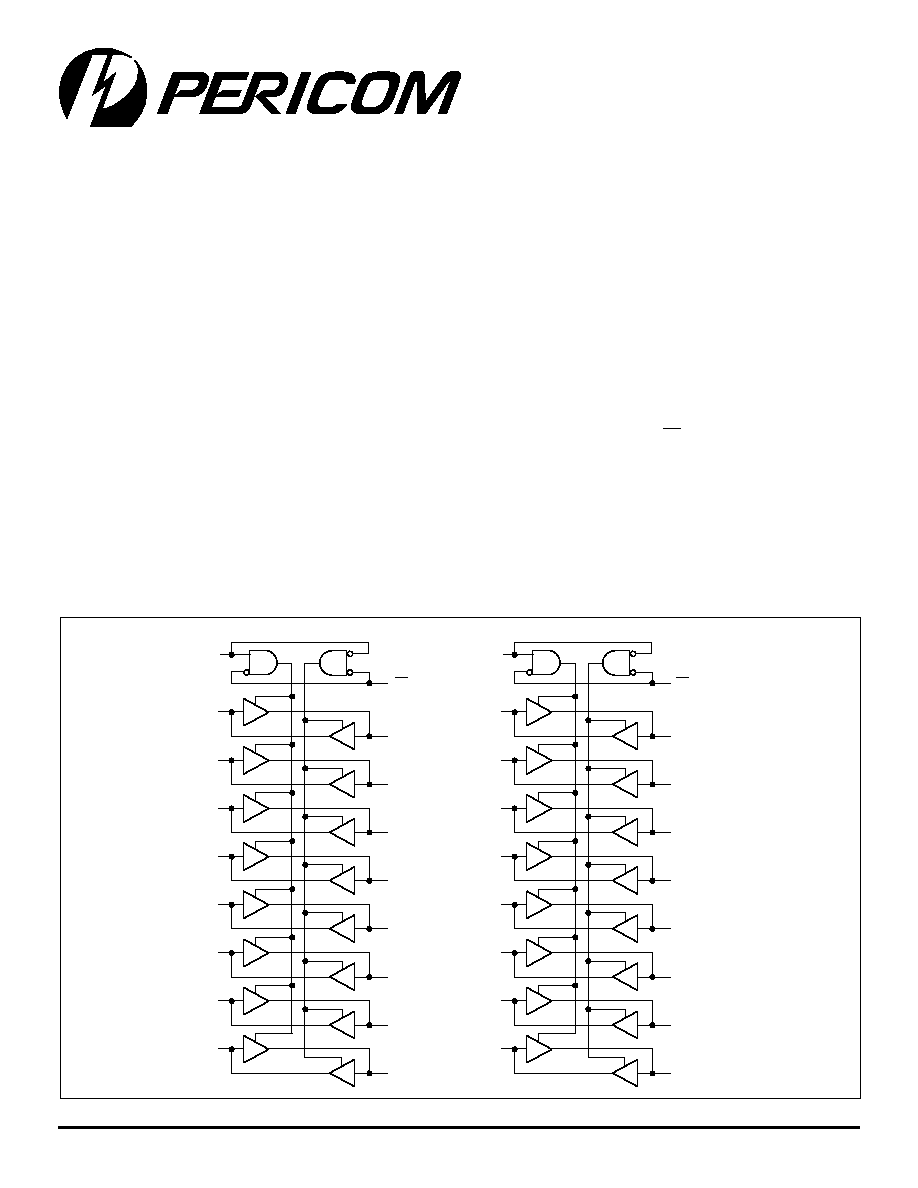
Logic Block Diagram
Product Features:
∑ Very high-speed bidirectional transceiver
for 150 pF heavy loads
∑ 16-bit switching in 5.5ns max
∑ Vcc = 5V ±10%
∑ Hysteresis on all inputs
∑ Balanced output drivers: ±24 mA
∑ Reduced system switching noise
∑ Typical V
OLP
(Output Ground Bounce) < 0.6V
at V
CC
= 5V, T
A
= 25∞C
∑ Packages available:
≠ 48-pin 240 mil wide plastic TSSOP (A)
≠ 48-pin 300 mil wide plastic SSOP (V)
∑ Device models available on request
1
B
0
1
A
0
1
OE
1
DIR
1
B
1
1
A
1
1
B
2
1
A
2
1
B
3
1
A
3
1
B
4
1
A
4
1
B
5
1
A
5
1
B
6
1
A
6
1
B
7
1
A
7
2
B
0
2
A
0
2
OE
2
DIR
2
B
1
2
A
1
2
B
2
2
A
2
2
B
3
2
A
3
2
B
4
2
A
4
2
B
5
2
A
5
2
B
6
2
A
6
2
B
7
2
A
7
PI74FCT162245MT
16-BIT BIDIRECTIONAL TRANSCEIVERS
2
PS2046A 03/12/96
12345678901234567890123456789012123456789012345678901234567890121234567890123456789012345678901212345678901234567890123456789012123456789012
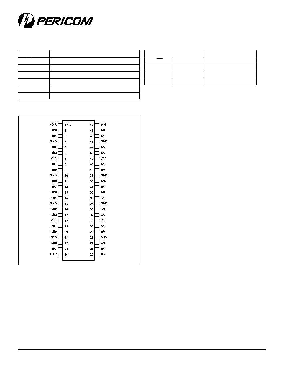
Product Pin Description
Pin Name
Description
xOE
Output Enable Inputs (Active LOW)
xDIR
Direction Control Input
xAx
Side A Inputs or 3-State Outputs
xBx
Side B Inputs or 3-State Outputs
GND
Ground
V
CC
Power
Inputs
(1)
X
OE
xDIR
Outputs
(1)
L
L
Bus B Data to Bus A
L
H
Bus A Data to Bus B
H
X
High Z State
Truth Table
Note: 1. H = High Voltage Level
X = Don't Care
L = Low Voltage Level
Z = High Impedance
Product Pin Configuration
48-PIN
V48
A48
PI74FCT162245MT
16-BIT BIDIRECTIONAL TRANSCEIVERS
3
PS2046A 03/12/96
12345678901234567890123456789012123456789012345678901234567890121234567890123456789012345678901212345678901234567890123456789012123456789012
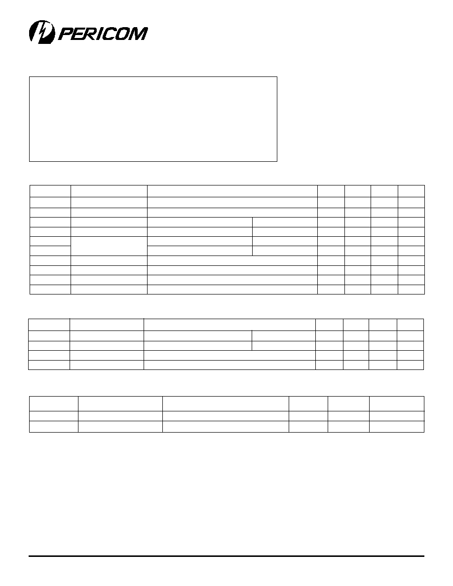
DC Electrical Characteristics
(Over the Operating Range, T
A
= ≠40∞C to +85∞C, V
CC
= 5.0V ± 10%)
Parameters Description
Test Conditions
(1)
Min.
Typ
(2)
Max.
Units
V
IH
Input HIGH Voltage
Guaranteed Logic HIGH Level
2.0
V
V
IL
Input LOW Voltage
Guaranteed Logic LOW Level
0.8
V
I
IH
Input HIGH Current
V
CC
= Max.
V
IN
= V
CC
1
µA
I
IL
Input LOW Current
V
CC
= Max.
V
IN
= GND
≠1
µA
I
OZH
High Impedance
V
CC
= Max.
V
OUT
= 2.7V
1
µA
I
OZL
Output Current
V
CC
= Max.
V
OUT
= 0.5V
≠1
µA
V
IK
Clamp Diode Voltage
V
CC
= Min., I
IN
= ≠18 mA
≠0.7
≠1.2
V
I
OS
Short Circuit Current
V
CC
= Max.
(3)
, V
OUT
= GND
≠80
≠140
≠200
mA
I
O
Output Drive Current
V
CC
= Max.
(3)
, V
OUT
= 2.5V
≠50
≠180
mA
V
H
Input Hysteresis
100
mV
Maximum Ratings
(Above which the useful life may be impaired. For user guidelines, not tested.)
Storage Temperature ................................................................. ≠65∞C to +150∞C
Ambient Temperature with Power Applied ................................. ≠40∞C to +85∞C
Supply Voltage to Ground Potential (Inputs & Vcc Only) .......... ≠0.5V to +7.0V
Supply Voltage to Ground Potential (Outputs & D/O Only) ....... ≠0.5V to +7.0V
DC Input Voltage ......................................................................... ≠0.5V to +7.0V
DC Output Current ................................................................................... 120 mA
Power Dissipation ......................................................................................... 1.0W
Note:
Stresses greater than those listed under
MAXIMUM RATINGS may cause permanent
damage to the device. This is a stress rating
only and functional operation of the device at
these or any other conditions above those
indicated in the operational sections of this
specification is not implied. Exposure to
absolute maximum rating conditions for
extended periods may affect reliability.
Output Drive Characteristics
(Over the Operating Range)
Parameters Description
Test Conditions
(1)
Min.
Typ
(2)
Max.
Units
V
OH
Output HIGH Voltage
V
CC
= Min., V
IN
= V
IH
or V
IL
I
OH
= ≠24.0 mA
2.4
3.3
V
V
OL
Output LOW Voltage
V
CC
= Min., V
IN
= V
IH
or V
IL
I
OL
= 24 mA
0.3
0.55
V
I
ODL
Output LOW Current
V
CC
= 5V, V
IN
= V
IH
OR
V
IL
, V
OUT
= 1.5V
(3)
60
115
150
mA
I
ODH
Output HIGH Current
V
CC
= 5V, V
IN
= V
IH
OR
V
IL
, V
OUT
= 1.5V
(3)
≠60
≠115
≠150
mA
Notes:
1. For Max. or Min. conditions, use appropriate value specified under Electrical Characteristics for the applicable device type.
2. Typical values are at Vcc = 5.0V, +25∞C ambient and maximum loading.
3. Not more than one output should be shorted at one time. Duration of the test should not exceed one second.
4. This parameter is determined by device characterization but is not production tested.
Capacitance
(T
A
= 25∞C, f = 1 MHz)
Parameters
(4)
Description
Test Conditions
Typ
Max.
Units
C
IN
Input Capacitance
V
IN
= 0V
4.5
6
pF
C
OUT
Output Capacitance
V
OUT
= 0V
5.5
8
pF
PI74FCT162245MT
16-BIT BIDIRECTIONAL TRANSCEIVERS
4
PS2046A 03/12/96
12345678901234567890123456789012123456789012345678901234567890121234567890123456789012345678901212345678901234567890123456789012123456789012
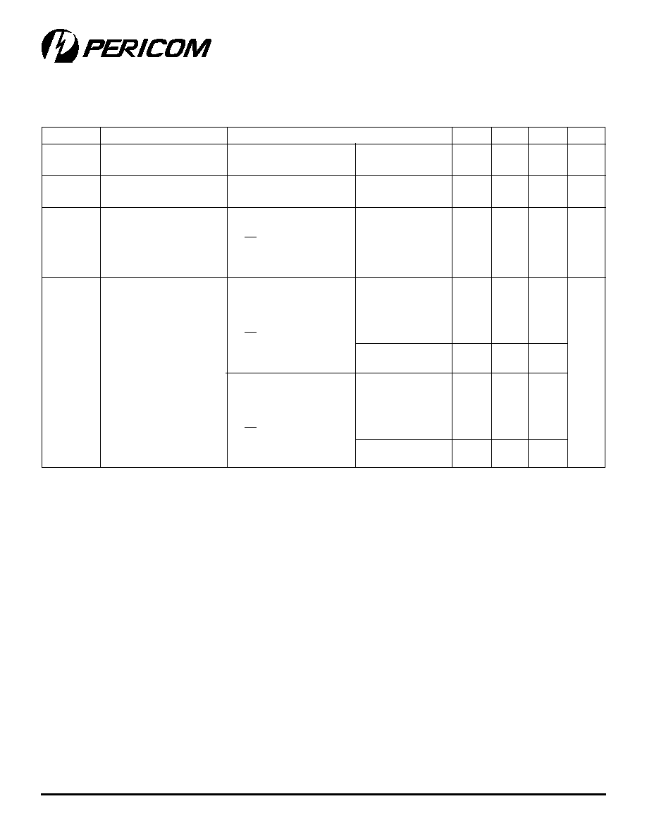
Power Supply Characteristics
Parameters Description
Test Conditions
(1)
Min.
Typ
(2)
Max.
Units
I
CC
Quiescent Power
V
CC
= Max.
V
IN
= GND or V
CC
0.1
500
µA
Supply Current
I
CC
Supply Current per
V
CC
= Max.
V
IN
= 3.4V
(3)
0.5
1.5
mA
Input @ TTL HIGH
I
CCD
Supply Current per
V
CC
= Max.,
V
IN
= V
CC
60
100
µA/
Input per MHz
(4)
Outputs Open
V
IN
= GND
MHz
X
OE = xDIR = GND
One Bit Toggling
50% Duty Cycle
I
C
Total Power Supply
V
CC
= Max.,
V
IN
= V
CC
0.6
1.5
(5)
mA
Current
(6)
Outputs Open
V
IN
= GND
f
I
= 10 MH
Z
50% Duty Cycle
X
OE = xDIR = GND
One Bit Toggling
V
IN
= 3.4V
0.9
2.3
(5)
V
IN
= GND
V
CC
= Max.,
V
IN
= V
CC
2.4
4.5
(5)
Outputs Open
V
IN
= GND
f
I
= 2.5 MH
Z
50% Duty Cycle
X
OE = xDIR = GND
16 Bits Toggling
V
IN
= 3.4V
6.4
16.5
(5)
V
IN
= GND
Notes:
1. For Max. or Min. conditions, use appropriate value specified under Electrical Characteristics for the applicable device.
2. Typical values are at Vcc = 5.0V, +25∞C ambient.
3. Per TTL driven input (V
IN
= 3.4V); all other inputs at Vcc or GND.
4. This parameter is not directly testable, but is derived for use in Total Power Supply Calculations.
5. Values for these conditions are examples of the Icc formula. These limits are guaranteed but not tested.
6. I
C
=I
QUIESCENT
+ I
INPUTS
+ I
DYNAMIC
I
C
= I
CC
+
I
CC
D
H
N
T
+ I
CCD
(f
CP
/2 + f
I
N
I
)
I
CC
= Quiescent Current
I
CC
= Power Supply Current for a TTL High Input (V
IN
= 3.4V)
D
H
= Duty Cycle for TTL Inputs High
N
T
= Number of TTL Inputs at D
H
I
CCD
= Dynamic Current Caused by an Input Transition Pair (HLH or LHL)
f
CP
= Clock Frequency for Register Devices (Zero for Non-Register Devices)
f
I
= Input Frequency
N
I
= Number of Inputs at f
I
All currents are in milliamps and all frequencies are in megahertz.
PI74FCT162245MT
16-BIT BIDIRECTIONAL TRANSCEIVERS
5
PS2046A 03/12/96
12345678901234567890123456789012123456789012345678901234567890121234567890123456789012345678901212345678901234567890123456789012123456789012
Notes:
1. See test circuit and wave forms.
2. Minimum limits are guaranteed but not tested on Propagation Delays.
3. This parameter is guaranteed but not production tested.
4. Skew between any two outputs, of the same package, switching in the same
direction. This parameter is guaranteed by design.
PI74FCT162245MT Switching Characteristics over Operating
Range -- High-Load Condition
162245MT
Com.
Parameters
Description
Conditions
(1)
Min
Max
Unit
t
PLH
Propagation Delay
(2)
C
L
= 150 pF
1.5
5.5
ns
t
PHL
X
A
X
to
X
B
X
All 16 Bits Switching
t
PZH
Output Enable Time
C
L
= 50 pF
1.5
6.2
ns
t
PZL
X
OE to
X
A
X
or
X
B
X
R
L
= 500
t
PHZ
Output Disable Time
(3)
1.5
5.6
ns
t
PLZ
X
OE to
X
A
X
or
X
B
X
t
SK
(o)
Output Skew
(4)
--
0.5
ns
Pericom Semiconductor Corporation
2380 Bering Drive ∑ San Jose, CA 95131 ∑ 1-800-435-2336 ∑ Fax (408) 435-1100 ∑ http://www.pericom.com