
1
PS2098B 11/
17
/02
12345678901234567890123456789012123456789012345678901234567890121234567890123456789012345678901212345678901234567890123456789012123456789012
12345678901234567890123456789012123456789012345678901234567890121234567890123456789012345678901212345678901234567890123456789012123456789012
12345678901234567890123456789012123456789012345678901234567890121234567890123456789012345678901212345678901234567890123456789012123456789012
PI74LCX244
Fast CMOS 3.3V 8-Bit Buffer/Line Driver
Product Features
∑ Functionally compatible with FCT3, LVT, and 74 series
244 families of products
∑ Tri-State outputs
∑ 5V Tolerant inputs and outputs
∑ 2.0V-3.6V V
CC
supply operation
∑ Balanced sink and source output drives (24 mA)
∑ Low ground bounce outputs
∑ Power Down High Impedance inputs and outputs
∑ Supports live insertion
∑ ESD Protection exceeds 2000V, Human Body Model
200V, Machine Model
∑ Packages available:
≠ 20-pin 209-mil wide plastic SSOP (H)
≠ 20-pin 173-mil wide plastic TSSOP (L)
≠ 20-pin 150-mil wide plastic QSOP (Q)
≠ 20-pin 300-mil wide plastic SOIC (S)
Product Description
Pericom Semiconductor's PI74LCX series of logic circuits are
produced using the Company's advanced 0.6 micron CMOS
technology achieving high speed while maintaining low power
operation.
The PI74LCX244 is an 8-bit non-inverting buffer/line driver designed
for driving high capacitive memory loads. With its balanced-drive
characteristics, this high-speed, low power device provides lower
ground bounce, transmission line matching of signals, fewer line
reflections and lower EMI and RFI effects. This makes it ideal for
driving on-board buses and transmission lines.
The PI74LCX244 can be driven from either 3.3V or 5.0V devices
allowing this device to be used as a translator in a mixed
3.3V/5.0V system.
Logic Block Diagram
Product Pin Configuration
Product Pin Description
Truth Table
(1)
Note:
1. H = High Voltage Level,
X = Don't Care,
L = Low Voltage Level,
Z = High Impedance
e
m
a
N
n
i
P
n
o
i
t
p
i
r
c
s
e
D
OE
A
E
O
,
B
e
l
b
a
n
E
t
u
p
t
u
O
e
t
a
t
S
-
3
)
W
O
L
e
v
it
c
A
(
s
t
u
p
n
I
D
XX
s
t
u
p
n
I
O
XX
s
t
u
p
t
u
O
D
N
G
d
n
u
o
r
G
V
CC
r
e
w
o
P
s
t
u
p
n
I
s
t
u
p
t
u
O
E
O
A
E
O
B
D
XX
O
XX
L
L
L
L
L
L
H
H
H
H
X
Z
1
2
3
4
5
6
7
8
9
10
20
19
18
17
16
15
14
13
12
11
VCC
OEB
OA0
DB0
OA1
DB1
OA2
DB2
OA3
DB3
OEA
DA0
OB0
DA1
OB1
DA2
OB2
DA3
OB3
GND
20-Pin
H20
L20
Q20
S20
OE
A
DA
0
OB
0
OB
1
DA
1
OB
2
DA
2
OB
3
DA
3
OA
0
DB
0
OE
B
OA
1
DB
1
OA
2
DB
2
OA
3
DB
3

2
PS2098B 11/
17
/02
12345678901234567890123456789012123456789012345678901234567890121234567890123456789012345678901212345678901234567890123456789012123456789012
12345678901234567890123456789012123456789012345678901234567890121234567890123456789012345678901212345678901234567890123456789012123456789012
PI74LCX244
3.3V 8-Bit Buffer/Line Driver
Maximum Ratings
(Above which the useful life may be impaired. For user guidelines, not tested.)
Note:
Stresses greater than those listed under
MAXIMUM RATINGS may cause permanent
damage to the device. This is a stress rating only and
functional operation of the device at these or any
other conditions above those indicated in the opera-
tional sections of this specification is not implied.
Exposure to absolute maximum rating conditions for
extended periods may affect reliability.
l
o
b
m
y
S
r
e
t
e
m
a
r
a
P
.
n
i
M
.
x
a
M
s
t
i
n
U
V
CC
e
g
a
tl
o
V
y
l
p
p
u
S
g
n
it
a
r
e
p
O
0
.
2
6
.
3
V
n
o
it
n
e
t
e
R
a
t
a
D
5
.
1
6
.
3
V
I
e
g
a
tl
o
V
t
u
p
n
I
0
5
.
5
V
O
e
g
a
tl
o
V
t
u
p
t
u
O
e
t
a
t
S
W
O
L
r
o
H
G
I
H
0
V
CC
e
t
a
t
S
-
I
R
T
0
5
.
5
I
OH
I
/
OL
t
n
e
r
r
u
C
t
u
p
t
u
O
V
CC
V
6
.
3
-
V
0
.
3
=
4
2
±
A
m
V
CC
V
7
.
2
=
2
1
±
T
A
e
r
u
t
a
r
e
p
m
e
T
g
n
it
a
r
e
p
O
r
i
A
-
e
e
r
F
-
0
4
5
8
+
∞
C
/t
V
e
t
a
R
e
g
d
E
t
u
p
n
I
V
,
V
0
.
2
-
V
8
.
0
=
V
CC
V
0
.
3
=
0
0
1
V
/
s
n
Recommended Operating Conditions
Storage Temperature ............................................................. ≠65∞C to +150∞C
Ambient Temperature with Power Applied ............................ ≠40∞C to +85∞C
Supply Voltage to Ground Potential (Inputs & Vcc Only)...... ≠0.5V to +7.0V
Supply Voltage to Ground Potential (Outputs & D/O Only) ..≠0.5V to +7.0V
DC Input Voltage ....................................................................≠0.5V to +7.0V
DC Output Current .............................................................................. 120 mA
Power Dissipation .................................................................................... 1.0W

3
PS2098B 11/
17
/02
12345678901234567890123456789012123456789012345678901234567890121234567890123456789012345678901212345678901234567890123456789012123456789012
12345678901234567890123456789012123456789012345678901234567890121234567890123456789012345678901212345678901234567890123456789012123456789012
PI74LCX244
3.3V 8-Bit Buffer/Line Driver
Notes:
1. For Max. or Min. conditions, use appropriate value specified under Electrical Characteristics for the applicable device type.
2. Typical values are at V
CC
= 3.3V, +25∞C ambient.
3. Per TTL driven input; all other inputs at Vcc or GND.
s
r
e
t
e
m
a
r
a
P
n
o
i
t
p
i
r
c
s
e
D
s
n
o
i
t
i
d
n
o
C
t
s
e
T
)
1
(
.
n
i
M
p
y
T
)
2
(
.
x
a
M
s
t
i
n
U
V
IH
e
g
a
tl
o
V
H
G
I
H
t
u
p
n
I
l
e
v
e
L
H
G
I
H
c
i
g
o
L
d
e
e
t
n
a
r
a
u
G
0
.
2
--
--
V
V
IL
e
g
a
tl
o
V
W
O
L
t
u
p
n
I
l
e
v
e
L
W
O
L
c
i
g
o
L
d
e
e
t
n
a
r
a
u
G
--
--
8
.
0
V
OH
e
g
a
tl
o
V
H
G
I
H
t
u
p
t
u
O
V
CC
6
.
3
-
7
.
2
=
I
OH
A
m
1
.
0
≠
=
V
CC
2
.
0
-
--
--
V
CC
7
.
2
=
I
OH
A
m
2
1
≠
=
2
.
2
--
--
V
CC
0
.
3
=
I
OH
A
m
8
1
≠
=
4
.
2
--
--
I
OH
A
m
4
2
≠
=
2
.
2
--
--
V
OL
e
g
a
tl
o
V
W
O
L
t
u
p
t
u
O
V
CC
6
.
3
-
7
.
2
=
I
OL
A
m
1
.
0
=
--
--
2
.
0
V
CC
7
.
2
=
I
OL
A
m
2
1
=
--
--
4
.
0
V
CC
0
.
3
=
I
OL
A
m
6
1
=
--
--
4
.
0
I
OL
A
m
4
2
=
--
--
5
5
.
0
V
IK
e
g
a
tl
o
V
e
d
o
i
D
p
m
a
l
C
V
CC
,.
n
i
M
=
I
IN
A
m
8
1
≠
=
--
-
7
.
0
-
2
.
1
I
I
t
n
e
r
r
u
C
e
g
a
k
a
e
L
t
u
p
n
I
0
V
I
V
5
.
5
6
.
3
-
7
.
2
=
c
c
V
--
--
5
±
A
µ
I
OZ
e
g
a
k
a
e
L
t
u
p
t
u
O
e
t
a
t
S
-
i
r
T
0
V
O
V
5
.
5
V
I
V
=
IH
V
r
o
IL
V
CC
6
.
3
-
7
.
2
=
--
--
5
±
I
OFF
e
l
b
a
s
i
D
n
w
o
D
r
e
w
o
P
V
CC
,
V
0
=
V
IN
V
r
o
OUT
V
5
.
5
--
--
0
1
I
CC
y
l
p
p
u
S
r
e
w
o
P
t
n
e
c
s
e
i
u
Q
t
n
e
r
r
u
C
V
CC
.
x
a
M
=
V
IN
V
r
o
D
N
G
=
CC
1
.
0
0
1
I
CC
y
l
p
p
u
S
r
e
w
o
P
t
n
e
c
s
e
i
u
Q
t
n
e
r
r
u
C
H
G
I
H
s
t
u
p
n
I
L
T
T
V
CC
.
x
a
M
=
V
IN
V
=
CC
V
6
.
0
≠
)
3
(
0
0
5
s
r
e
t
e
m
a
r
a
P
n
o
i
t
p
i
r
c
s
e
D
s
n
o
i
t
i
d
n
o
C
t
s
e
T
.
p
y
T
s
t
i
n
U
C
IN
e
c
n
a
ti
c
a
p
a
C
t
u
p
n
I
V
CC
V
,
n
e
p
O
=
I
V
r
o
V
0
=
CC
7
F
p
C
OUT
e
c
n
a
ti
c
a
p
a
C
t
u
p
t
u
O
V
CC
V
,
V
3
.
3
=
I
V
r
o
V
0
=
CC
8
C
PD
e
c
n
a
ti
c
a
p
a
C
n
o
it
a
p
i
s
s
i
D
r
e
w
o
P
V
CC
V
,
V
3
.
3
=
I
V
r
o
V
0
=
CC
,
z
H
M
0
1
=
F
5
2
Capacitance
DC Electrical Characteristics
(Over the Operating Range, T
A
=
-
40∞C to +85∞C, V
CC
= 2.7V to 3.6V)
4
PS2098B 11/
17
/02
12345678901234567890123456789012123456789012345678901234567890121234567890123456789012345678901212345678901234567890123456789012123456789012
12345678901234567890123456789012123456789012345678901234567890121234567890123456789012345678901212345678901234567890123456789012123456789012
PI74LCX244
3.3V 8-Bit Buffer/Line Driver
Switching Characteristics over Operating Range
Note:
1. Skew between any two outputs, of the same package, switching in the same direction.
Dynamic Switching Characteristics
(T
A
= +25∞C)
Note:
1. Measured with n≠1 outputs switching from High-to-Low or Low-to-High. The remaining output is measured in the LOW state.
s
r
e
t
e
m
a
r
a
P
n
o
i
t
p
i
r
c
s
e
D
s
n
o
i
t
i
d
n
o
C
V
CC
V
3
.
0
±
V
3
.
3
=
V
CC
V
7
.
2
=
s
t
i
n
U
.
n
i
M
.
x
a
M
.
n
i
M
.
x
a
M
t
PLH
t
PHL
y
a
l
e
D
n
o
it
a
g
a
p
o
r
P
D
XX
O
o
t
XX
C
L
F
p
0
5
=
R
L
0
0
5
=
5
.
1
5
.
6
5
.
1
5
.
7
s
n
t
PZH
t
PZL
e
m
it
e
l
b
a
n
E
t
u
p
t
u
O
5
.
1
0
.
8
5
.
1
0
.
9
t
PHZ
t
PLZ
e
m
i
T
e
l
b
a
s
i
D
t
u
p
t
u
O
5
.
1
0
.
7
5
.
1
0
.
8
t
SK
(
O
)
w
e
k
S
t
u
p
t
u
O
)
1
(
0
.
1
s
r
e
t
e
m
a
r
a
P
n
o
i
t
p
i
r
c
s
e
D
s
n
o
i
t
i
d
n
o
C
t
s
e
T
)
1
(
.
p
y
T
s
t
i
n
U
V
OLP
e
g
a
tl
o
V
k
a
e
P
W
O
L
c
i
m
a
n
y
D
V
CC
C
,
V
3
.
3
=
L
F
p
0
5
=
V
IH
V
,
V
3
.
3
=
IL
V
0
=
8
.
0
V
V
OLV
e
g
a
tl
o
V
y
e
ll
a
V
W
O
L
c
i
m
a
n
y
D
V
CC
C
,
V
3
.
3
=
L
F
p
0
5
=
V
IH
V
,
V
3
.
3
=
IL
V
0
=
5
PS2098B 11/
17
/02
12345678901234567890123456789012123456789012345678901234567890121234567890123456789012345678901212345678901234567890123456789012123456789012
12345678901234567890123456789012123456789012345678901234567890121234567890123456789012345678901212345678901234567890123456789012123456789012
PI74LCX244
3.3V 8-Bit Buffer/Line Driver
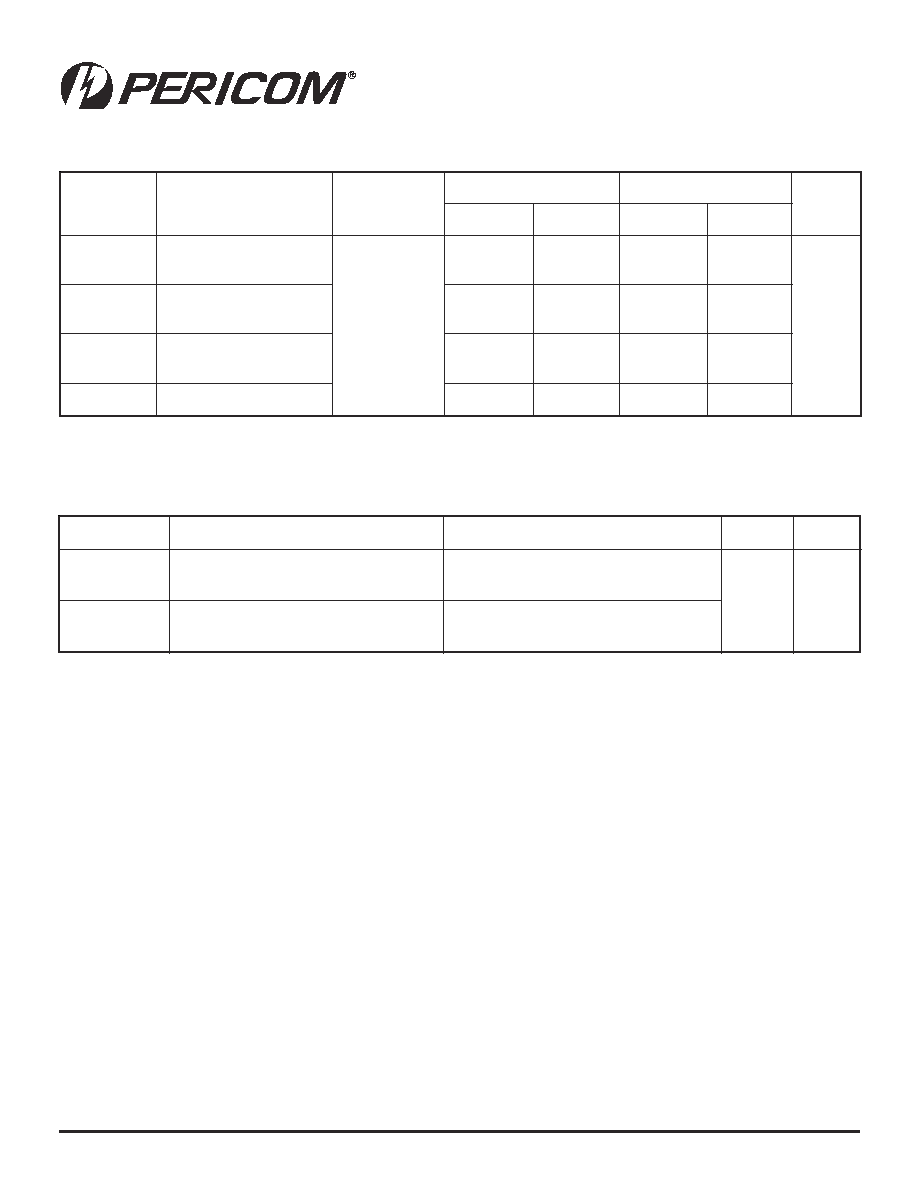
Packaging Mechanical: 20-pin SSOP (H-package)
Packaging Mechanical: 20-pin TSSOP (L-package)
.272
.295
.078
.002
SEATING
PLANE
.0098
Max.
.0256
BSC
.022
.037
.004
.009
.291
.322
1
20
.197
.220
0.25
X.XX
X.XX
DENOTES DIMENSIONS
IN MILLIMETERS
0.050
7.40
8.20
0.55
0.95
0.09
0.25
5.00
5.60
2.00
6.90
7.50
0.65
Max
Min
.252
.260
.047
1.20
.002
.006
SEATING
PLANE
.0256
BSC
.018
.030
.004
.008
.238
.269
1
20
.169
.177
X.XX
X.XX
DENOTES CONTROLLING
DIMENSIONS IN MILLIMETERS
0.05
0.15
6.1
6.7
0.45
0.75
0.09
0.20
4.3
4.5
6.4
6.6
0.65
0.19
0.30
.007
.012
Max

6
PS2098B 11/17/02
12345678901234567890123456789012123456789012345678901234567890121234567890123456789012345678901212345678901234567890123456789012123456789012
12345678901234567890123456789012123456789012345678901234567890121234567890123456789012345678901212345678901234567890123456789012123456789012
PI74LCX244
3.3V 8-Bit Buffer/Line Driver
Pericom Semiconductor Corporation
2380 Bering Drive ∑ San Jose, CA 95131 ∑ 1-800-435-2336 ∑ Fax (408) 435-1100 ∑ http://www.pericom.com
SEATING
PLANE
.050
BSC
1
20
0-8∞
.2914
.2992
X.XX
X.XX
DENOTES CONTROLLING
DIMENSIONS IN MILLIMETERS
7.40
7.60
.496
.511
12.60
12.99
1.27
.0926
.1043
2.35
2.65
.394
.419
10.00
10.65
.0040
.0118
0.10
0.30
.013
.020
0.33
0.51
.010
.029
0.254
0.737
.0091
.0125
0.23
0.32
0.41
1.27
.016
.050
x 45∞
.020
.030
0.508
0.762
REF
Ordering Information
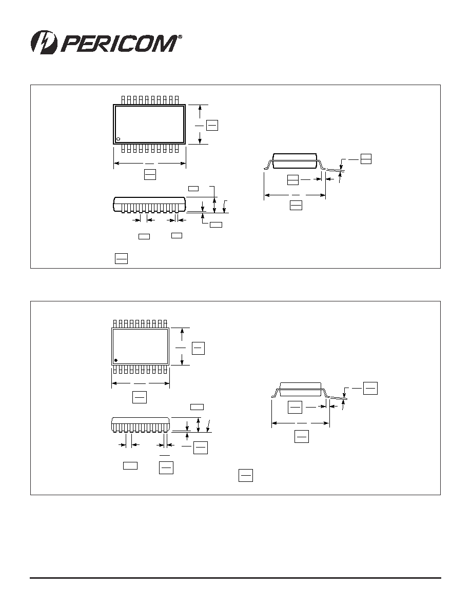
Packaging Mechanical: 20-pin QSOP (Q-package)
Packaging Mechanical : 20-pin SOIC (S-package)
.337
.344
.053
.069
.004
.010
SEATING
PLANE
.025
BSC
.007
.010
.228
.244
.150
.157
1
20
.016
.050
X.XX
X.XX
DENOTES DIMENSIONS
IN MILLIMETERS
0.635
8.56
8.74
1.35
1.75
5.79
6.19
0.41
1.27
0.101
0.254
.008
.012
0.203
0.305
3.81
3.99
0.178
0.254
.058
1.47
.015 x 45∞
0.38
REF
Detail A
Detail A
.008
0.20
MIN.
Guage Plane
.010
0.254
.041
1.04
REF
.016
.035
0.41
0.89
0∞-6∞
.008
.013
0.20
0.33
e
d
o
C
g
n
i
r
e
d
r
O
n
o
i
t
p
i
r
c
s
e
D
H
4
4
2
X
C
L
4
7
I
P
)
H
(
P
O
S
S
c
it
s
a
l
P
e
d
i
w
li
m
-
9
0
2
n
i
P
-
0
2
L
4
4
2
X
C
L
4
7
I
P
)
L
(
P
O
S
S
T
c
it
s
a
l
P
e
d
i
w
li
m
-
3
7
1
n
i
P
-
0
2
Q
4
4
2
X
C
L
4
7
I
P
)
Q
(
P
O
S
Q
c
it
s
a
l
P
e
d
i
w
li
m
-
0
5
1
n
i
P
-
0
2
S
4
4
2
X
C
L
4
7
I
P
)
S
(
P
O
S
S
c
it
s
a
l
P
e
d
i
w
li
m
-
0
0
3
n
i
P
-
0
2