
1
PS8636B 07/26/04
Features
∑ PI74 SSTU32864 is designed for low-voltage operation,
V
DD
= 1.8V
∑ Supports Low Power Standby Operation
∑ All Inputs are SSTL_18 Compatible, except RST, C0, C1,
which are LVCMOS.
∑ Output drivers are optimized to drive DDR-II DIMM loads
∑ Designed for DDR Memory
∑ Packaging (Pb-free & Green available):
-96 Ball LFBGA (NB)
Block Diagram 1:2 Mode (Positive Logic)
PI74SSTU32864
25-Bit 1:1 or 14-Bit 1:2 Configurable
Registered Buffer
TO OTHER CHANNELS
CK
CK
RST
1D
C1
R
QCKEA
QCKEB*
QODTA
1D
C1
R
Q1A
Q1B*
QCSB*
QCSA
1D
C1
R
1D
C1
R
QODTB*
V
REF
DCKE
DODT
DCS
CSR
D1
Note: Disabled in 1:1 configuration
0
1
Description
Pericom Semiconductor's PI74SSTU32864 logic circuit is produced
using advanced CMOS technology. This 25-Bit 1:1 or 14-Bit 1:2
configurable registered buffer is designed for 1.7V to 1.9V V
DD
operation.
All clock and data inputs are compatible with the JEDEC standard
for SSTL_18. The control inputs are LVCMOS. All outputs are
1.8V LVCMOS drivers that have been optimized to drive the
DDR-II DIMM load.
The SSTU32864 operates from a differential clock (CK and CK).
Data is registered at the crossing of CK going high, and CK going
low.
The C0 input controls the pinout configuration of the 1:2 pinout
from A configuration (when LOW) to B configuration (when
HIGH). The C1 input controls the pinout configuration for 25-Bit
1:1 (when LOW) to 14-Bit 1:2 (when HIGH).
The device supports low-power standby operation. When the reset
input (RST) is low, the differential input receivers are disabled and
undriven (floating) data, clock and reference voltage (V
REF
) inputs
are allowed. In addition , when RST is low, all registers are reset,
and all outputs are forced low. The LVCMOS RST and Cn inputs
must always be held at a valid logic high or low level.
To ensure defined outputs from the register before a stable clock has
been supplied, RST must be held in the low state during power up.
In the DDR-II RDIMM application, RST is specified to be completely
asynchronous with respect to CK and CK. Therefore, no timing
relationship can be guaranteed between the two. When entering
reset, the register will be cleared and the outputs will be driven
low quickly, relative to the time to disable the differential input
receivers. However, when coming out of reset, the register will
become active quickly, relative to the time to enable the differential
input receivers.
As long as the data inputs are low, and the clock is stable during
the time from the low-to-high transition of RST until the input
receivers are fully enabled, the design of the SSTU32864 must
ensure that the outputs remain low, thus ensuring no glitches on
the output.
The device monitors both DCS and CSR inputs and will gate the
Qn outputs from changing states when both DCS and CSR inputs
are high. If either DCS or CSR input is low, the Qn outputs will
function normally. The RST input has priority over the DCS and CSR
control will force the outputs low. If the DCS control functionality
is not desired, then the CSR input can be hardwired to ground,
in which case, the set-up time requirement for DCS would be the
same as for the other D data inputs.
2
PS8636B 07/26/04
PI74SSTU32864
25-Bit 1:1 or 14-Bit 1:2
Configurable Buffer
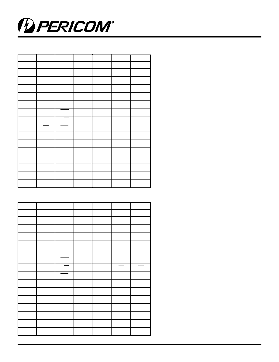
Pin Configuration 1:2 Register (C0 = 0, C1 = 1)
1
2
3
4
5
6
A
DCKE
NC
V
REF
V
DD
QCKEA QCKEB
B
D2
NC
GND
GND
Q2A
Q2B
C
D3
NC
V
DD
V
DD
Q3A
QODTB
D
DODT
NC
GND
GND
QODTA
Q4B
E
D5
NC
V
DD
V
DD
Q5A
Q5B
F
D6
NC
GND
GND
Q6A
Q6B
G
NC
RST
V
DD
V
DD
C1
C0
H
CK
DCS
GND
GND
QCSA
QCSB
J
CK
CSR
V
DD
V
DD
ZOH
ZOL
K
D8
NC
GND
GND
Q8A
Q8B
L
D9
NC
V
DD
V
DD
Q9A
Q9B
M
D10
NC
GND
GND
Q10A
Q10B
N
D11
NC
V
DD
V
DD
Q11A
Q11B
P
D12
NC
GND
GND
Q12A
Q12B
R
D13
NC
V
DD
V
DD
Q13A
Q13B
T
D14
NC
V
REF
V
DD
Q14A
Q14B
Pin Configuration 1:1 Register (C0 = 0, C1 = 0)
1
2
3
4
5
6
A
DCKE
NC
V
REF
V
DD
QCKE
NC
B
D2
D15
GND
GND
Q2
Q15
C
D3
D16
V
DD
V
DD
Q3
Q15
D
DODT
NC
GND
GND
QODT
NC
E
D5
D17
V
DD
V
DD
Q5
Q17
F
D6
D18
GND
GND
Q6
Q18
G
NC
RST
V
DD
V
DD
C1
C0
H
CK
DCS
GND
GND
QCS
NC
J
CK
CSR
V
DD
V
DD
ZOH
ZOL
K
D8
D19
GND
GND
Q8
Q19
L
D9
D20
V
DD
V
DD
Q9
Q20
M
D10
D21
GND
GND
Q10
Q21
N
D11
D22
V
DD
V
DD
Q11
Q22
P
D12
D23
GND
GND
Q12
Q23
R
D13
D24
V
DD
V
DD
Q13
Q24
T
D14
D25
V
REF
V
DD
Q14
Q25

3
PS8636B 07/26/04
PI74SSTU32864
25-Bit 1:1 or 14-Bit 1:2
Configurable Buffer
Pin Configuration 1:2 Register (C0 = 1, C1 = 1)
1
2
3
4
5
6
A
D1
NC
V
REF
V
DD
Q1A
QB
B
D2
NC
GND
GND
Q2A
Q2B
C
D3
NC
V
DD
V
DD
Q3A
Q3B
D
D4
NC
GND
GND
Q4A
Q4B
E
D5
NC
V
DD
V
DD
Q5A
Q5B
F
D6
NC
GND
GND
Q6A
Q6B
G
NC
RST
V
DD
V
DD
C1
C0
H
CK
DCS
GND
GND
QCSA
QCSB
J
CK
CSR
V
DD
V
DD
ZOH
ZOL
K
D8
NC
GND
GND
Q8A
Q8B
L
D9
NC
V
DD
V
DD
Q9A
Q9B
M
D10
NC
GND
GND
Q10A
Q10B
N
DODT
NC
V
DD
V
DD
QODTA QODTB
P
D12
NC
GND
GND
Q12A
Q12B
R
D13
NC
V
DD
V
DD
Q13A
Q13B
T
DCKE
NC
V
REF
V
DD
QCKEA QCKEB
NB 96-ball LFBGA (MO-205CC) Top View

4
PS8636B 07/26/04
PI74SSTU32864
25-Bit 1:1 or 14-Bit 1:2
Configurable Buffer
Terminal Functions
Name
Description
Characteristics
GND
Ground
Ground Input
V
DD
Power Supply
1.8V nominal
V
REF
Input Reference Voltage
0.9V nominal
Z
OH
Reserved for future use
Input
Z
OL
Reserved for future use
Input
CK
Positive master clock input
Differential Clock input
CK
Negative master clock input
Differential Clock input
C0, C1
Configuration control inputs
LVCMOS inputs
RST
Asynchronous reset input - resets registers and disables V
REF
data and clock differen-
tial - input receivers
LVCMOS inputs
CSR, DCS Chip select inputs disables D1-D24 outputs switching when both inputs are high
SSTL_18 input
D1, D25
Data input - clocked in on the crossing of the rising edge of CK and the falling edge
of CK
SSTL_18 input
DODT
The outputs of this register bit will not be suspended by the DCS and CSR control
SSTL_18 input
DCKE
The outputs of this register bit will not be suspended by the DCS and CSR control
SSTL_18 input
Q1-Q25
Data outputs that are suspended by the DCS and CSR control
1.8V CMOS
QCS
Data output that will not be suspended by the DCS and CSR controll
1.8V CMOS
QODT
Data output that will not be suspended by the DCS and CSR controll
1.8V CMOS
QCKE
Data output that will not be suspended by the DCS and CSR controll
1.8V CMOS
Function Table (each flip flop)
Inputs
Outputs
RST
DCS
CSR
CK
CK
Dn, DODT,
DCKE
Qn
QCS
QODT,
QCKE
H
L
L
L
L
L
L
H
L
L
H
H
L
H
H
L
L
L or H
L or H
X
Q0
Q0
Q0
H
L
H
L
L
L
L
H
L
H
H
H
L
H
H
L
H
L or H
L or H
X
Q0
Q0
Q0
H
H
L
L
L
H
L
H
H
L
H
H
H
H
H
H
L
L or H
L or H
X
Q0
Q0
Q0
H
H
H
L
Q0
H
L
H
H
H
H
Q0
H
H
H
H
H
L or H
L or H
X
Q0
Q0
Q0
L
X or floating X or floating X or floating X or floating X or floating
L
L
L

5
PS8636B 07/26/04
PI74SSTU32864
25-Bit 1:1 or 14-Bit 1:2
Configurable Buffer
Notes:
1. The RST and Cn inputs of the device must be held at valid levels (not floating) to ensure proper device operation. The differential inputs must
not be floating, unless RST is low.
Notes:
1. Stresses greater than those listed under MAXIMUM
RAINGS may cause permanent damage to the device.
This is a stress rating only and functional operation of the
device at these or any other conditions above those indi-
cated in the operational sections of this specification is not
implied. Exposure to absolute maximum rating conditions
for extended periods may affect reliability.
2. The input and output negative-voltage ratings may be ex-
ceeded if the input and output clamp-current ratings are
observed.
3. This value is limited to 2.5V maximum
Maximum Ratings
(Above which the useful life may be impaired. For user guidelines, not tested.)
Storage Temperature ................................................... ≠65∞C to +150∞C
Supply Voltage Range, V
DD
.............................................≠0.5V to 2.5V
Input Voltage Range,V
I
: (See Notes 2 and 3): ................≠0.5V to 2.5V
Output Voltage Range, V
O
(See Notes 2 and 3)....≠0.5V to V
DD
+ 0.5V
Input Clamp current, I
IK
(V
I
< 0 or V
I
= VDD )......................... ≠50mA
Output Clamp current, I
OK
(V
O
< 0 or V
O
> VDD).................... ±50mA
Continous Output Current, I
O
(V
O
= 0 to VDD) ........................ ±50mA
Continous Current through each V
DD
or GND......................... ±100mA
Recommended Operating Conditions
(1)
Parameters
Descrition
Min.
Nom.
Max.
Units
V
DD
Supply Voltage
1.7
1.9
V
V
REF
Reference Voltage
0.49 x V
DD
0.50 x V
DD
0.51 x V
DD
V
TT
Termination Voltage
V
REF
-40mA
V
REF
V
REF
-40mA
V
I
Input Voltage
0
V
DD
V
IH
AC High - Level Input Voltage
Data
Inputs
V
REF
250mV
V
IL
AC Low- Level Input Voltage
V
REF
-250mV
V
IH
DC High - Level Input Voltage
V
REF
125mV
V
IL
DC Low- Level Input Voltage
V
REF
-125mV
V
IH
High Level Input Voltage
RST, CN
0.65 x V
DD
V
IL
Low Level Input Voltage
0.35 x V
DD
V
ICR
Common-mode input Voltage
CK, CK
0.675
1.125
V
ID
Differential Input Voltage
600
mV
I
OH
High-Level Output Current
-8
mA
I
OL
Low-Level Output Current
-8
T
A
Operating Free-air Temperature
0
70
∫C

6
PS8636B 07/26/04
PI74SSTU32864
25-Bit 1:1 or 14-Bit 1:2
Configurable Buffer
Notes
1. This parameter is not necessarily production tested.
2. Data and V
REF
inputs must be a low minimum time of t
act
max, after RST is taken high.
3. Data and clock inputs must be held at valid levels (not floating) a minimum time of t
inact
max after RST is taken low.
Timing Requirements
Over Recommended Operating Free Air Temperature range (See Figure 1)
Parameter
Description
Min.
Max
Units
f
clock
Clock frequency
270
MHz
t
W
Pulse Duration, CK, CK, High or low
1
ns
t
act
(1)
Differential inputs active time
(1)
10
t
inact
(1)
Differential inputs inactive time
(2)
15
t
su
Setup time
DCS before CK, CK, CSR high
0.7
DCS before CK, CK, CSR low
0.5
CSR DODT, CKE anddata before CK, CK
0.5
th
Hold Time
DCS, CSR DODT, CKE adn data before CK, CK
0.5
Notes:
1. The vendor must supply this value for full device description.
Electrical Characteristics
Over Recommended Operating Free Air Temperature range
Parameters
Description
Test Conditions
V
DD
Min. Nom. Max. Units
V
OH
I
OH
= -6 mA
1.7V
1.2
V
V
OL
I
OL
= 6 mA
1.7V
0.5
I
I
All inputs
V
I
= V
DD
or GND
±5
µA
I
DD
Static Stand-by
RST = GND
I
O
= 0
1.9V
100
Static Operating
RST = V
DD,
V
I =
V
IH(AC)
or V
IL(AC)
40
mA
I
DDD
Dynamic Operating
Clock only
RST = V
DD
, V
I
= V
IH(AC),
or
V
IL(AC)
CK and CK switching 50%
duty cycle
1.8V
28
µA/
clock
MHz
Dynamic Operating - per
each data input, 1:1 mode
RST = V
DD
, V
I
= V
IH(AC),
or
V
IL(AC)
CK and CK switching 50%
duty cycle. One data input switch-
ing at half clock frequency, 50%
duty cycle
18
µA/
clock
MHz
data
input
Dynamic Operating - per
each data input, 1:2 mode
RST = V
DD
, V
I
= V
IH(AC),
or
V
IL(AC)
CK and CK switching 50%
duty cycle. One data input switch-
ing at half clock frequency, 50%
duty cycle
36
C
I
Data inputsp
V
I
= V
REF
±250mV
2.5
3.5
pF
CK and CK
V
ICR
= 0.9V, V
ID
= 600mV
2
3
RST
V
I
= V
DD
or GND
2.5

7
PS8636B 07/26/04
PI74SSTU32864
25-Bit 1:1 or 14-Bit 1:2
Configurable Buffer
Notes:
1. Difference between dV/dt_r (rising edge rate) and dV/dt_f (falling edge rate).
Output Edge Rates
Over Recommended Operating Free Air Temperature range (See Figure 2)
Parameters
V
DD
= 1.8V ± 0.1V
Units
Min.
Max.
dV/dt_r
1
4
V/ns
dV/dt_f
1
4
dV/dt
(1)
1
Note:
1. Includes 350ps test load transmission-line delay.
2. This parameter is not necessarily production tested.
3. For reference only. Final values to be determined.
Switching Characteristics
Over Recommended Operating Free Air Temperature range (See Figure 1)
Parameters
From
(Input)
To
(Output)
V
DD
= 1.8V ± 0.1V
Units
Min.
Max.
f
max
270
MHz
t
pdm
CK and CK
Q
1.41
(3)
2.15
(3)
ns
tpdmss
(simultaneous switching)
(1, 2)
CK and CK
Q
2.35
(3)
t
RPHL
RST
Q
0
3

8
PS8636B 07/26/04
PI74SSTU32864
25-Bit 1:1 or 14-Bit 1:2
Configurable Buffer
Voltage and Current Waveforms
Input Active and Inactive Times
Voltage Waveforms - Pulse Duration
Voltage Waveforms - Setup and Hold Times
Test Circuit and Switching Waveforms
Figure 1. Parameter Measurement Information (V
DD
= 1.8V ± 0.1V)
Load Circuit
Voltage Waveforms - Propagation Delay Times
Voltage Waveforms - Propagation Delay Times
Output
V
ICR
t
PLH
t
PHL
V
ICR
V
ID
V
OH
V
TT
V
TT
V
OL
CK
CK
LVCMOS
RST
Input
I
DD(2)
V
DD
V
DD
/2
t
inact
0V
10%
90%
t
act
V
DD
/2
LVCMOS
RESET
Input
Output
tRPHL
V
DD
/2
V
OH
V
IH
V
IL
V
TT
V
OL
Input
V
ICR
V
ICR
t
w
V
ID
Input
CK
CK
th
tsu
VIL
VICR
VREF
VREF
VID
VIH
TL= 350ps, 50-ohm
R = 1000-ohm
VDD
CL= 30pF
(see note 1)
CK
CK
DUT
RL= 100-ohm
Test Point
Test Point
Test Point
CK Inputs
TL= 50-ohm
R = 1000-ohm
Out
Notes:
1. C
L
includes probe and jig capacitance
2. I
DD
tested with clock and data inputs held at V
DD
or GND and I
O
= 0mA
3. All input pulses are supplied by generators having the following characteristics: Pulse Repertition Rate 10 MHz, ZO = 50, input slew
rate = 1V/ns ± 20% (unless otherwise specified).
4. The outputs are measured one at a time with one transition per measurement.
5. V
REF
= V
DD
/2
6. V
IH
= V
REF
+250mV (ac voltage levels) for differential inputs. V
IH
= V
DD
for LVCMOS input.
7. V
IL
= V
REF
-250mV (ac voltage levels) for differential inputs. V
IL
= GND
for LVCMOS input.
8. V
ID
= 600mV
9. t
PLH
and t
PHL
are the same as t
pdm.

9
PS8636B 07/26/04
PI74SSTU32864
25-Bit 1:1 or 14-Bit 1:2
Configurable Buffer
R = 50-ohm
VDD
CL= 10pF
(see note 1)
DUT
Test Point
Out
Output
80%
20%
dt_f
V
OL
V
OH
dv_f
RL = 50-ohm
CL= 10pF
(see note 1)
DUT
Test Point
Out
Output
80%
20%
VOL
VOH
dv_r
dv_r
Load Circuit -High -to- Low Slew Rate Measurement
Load Circuit - Low -to- High Slew Rate Measurement
Voltage Waveforms - High -to- Low Slew Rate Measurement
Voltage Waveforms - Low -to- High Slew Rate Measurement
Figure 2. Output Slew-Rate Measurement Information (V
DD
= 1.8V ± 0.1V)
Notes:
1. C
L
includes probe and jig capacitance
2. All input pulses are supplied by generators having the following characteristics: PRR 10MHz, ZO = 50, input slew rate = 1 V/ns ± 20%
(unless otherwise specified).

10
PS8636B 07/26/04
PI74SSTU32864
25-Bit 1:1 or 14-Bit 1:2
Configurable Buffer
Packaging Mechanical: 96-ball LFBGA (NB)
Pericom Semiconductor Corporation ∑ 1-800-435-2336 ∑ www.pericom.com
Ordering Information
Notes:
1. Thermal characteristics can be found on the company web site at www.pericom.com/packaging/
2. Number of Transistors = TBD
Ordering Code
Package Code
Package Type
PI74SSTU32864NB
NB
96-Ball LFBGA
PI74SSTU32864NBE
NB
Pb-free & Green, 96-Ball LFBGA