 | –≠–ª–µ–∫—Ç—Ä–æ–Ω–Ω—ã–π –∫–æ–º–ø–æ–Ω–µ–Ω—Ç: GP-488 | –°–∫–∞—á–∞—Ç—å:  PDF PDF  ZIP ZIP |

PerkinElmer Optoelectronics
page 3
P
erkinElmer's Mini-Triggered
Spark Gaps are designed for high relia-
bility switching up to 4 kV and 10 kA.
Constructed of hermetically sealed
ceramic-metal, filled with pressurized
gas, they are typically used for activating
electro-explosive devices such as
exploding bridgewires, electronic
safe and arm systems, and detonators.
PerkinElmer's Trigger Transformers are
matched to the requirements of the
Mini-Triggered Spark Gaps to provide
a high voltage pulse with a fast rise
time and low current. PerkinElmer
Trigger Transformers are designed
to be the most durable and reliable
transformers available.
Features
∑
High reliability
∑
Extremely low jitter
∑
Environmentally durable
∑
Small size
∑
Matching trigger transformers
EVERYTHING
IN A
NEW
LIGHT.
Mini-Triggered
Spark Gaps
and Transformers
page 2
PerkinElmer Optoelectronics
Miniature Triggered
Spark Gaps
The triggered spark gap is a three
element, gas-filled, ceramic-to-metal,
hermetically sealed, pressurized
switch that operates in an arc dis-
charge mode, conducting moderately
high peak currents for short dura-
tions. Commutation between two
main electrodes is initiated by a
trigger pulse.
Applications
Precision timing and firing for in-flight
functions such as rocket motor igni-
tion, warhead detonation and missile
stage separation. Each of these
applications involves the activation
of electro-explosive devices such as:
∑
Exploding bridgewire (EBW)
∑
Exploding foil initiator (EFI)
∑
Electronic safe and arm (ESA)
∑
Slapper/detonator
These compact small, rugged gaps
were designed for high-reliability
applications where size, switch
speed, and ability to withstand
rugged missile environmental condi-
tions of extreme shock, temperature,
and vibration are required. They are
designed for switching peak currents
up to 10kA at operating voltages
from 2.0 to 4.0 kV with reliable
triggering voltage of 2kV. Prefires
and failure to fire have been fully
evaluated in the basic gap designs.
Switching speeds of 70ns with trigger
pulse energies as low as 500 micro-
joules is typical.
Performance
Characteristics
Electrical characteristics are
determined by testing in the circuit
shown in Figure 1. The output circuit
consisting of the switch, a 0.2 µF
capacitor, and a 0.25 ohm current
viewing resistor (CVR) is typical for life
testing. It closely matches the condi-
tions found in many typically used
circuits. For function testing, the 0.25
ohm CVR is replaced with a 0.005
ohm CVR.
Typical data taken with a 0.005 ohm
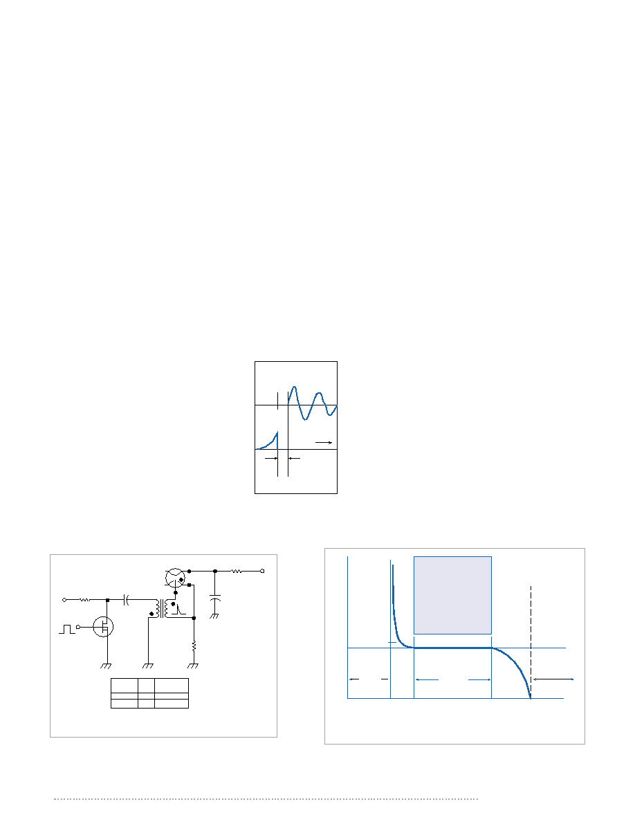
CVR are shown in Figure 2. This
curve contains traces of the trigger
voltage and conduction current. First,
the trigger voltage rises to the point
of trigger breakdown. Then there is a
period designated "turn-on" or delay
time during which the arc is forming
followed by main gap conduction.
This delay time varies from 50 to
1500 ns depending on gap operating
voltage, trigger mode, amplitude and
pulse width.
2N6798
VT(IN)
1.0 m
CT
TR
CVR
0.2
µ
F
2.4-3.5 KV
5 m
GAP
OE
AE
T
+
+
--
+
VT(IN)
Volts DC
20-40
100-200
CT
µ
F
2.2
0.10
XFMR
TR-2189/2206
TR-2190/2207
Figure 1. Triggered Spark Gap Test Circuit
Trigger
Voltage
Time
Turn-on
Time
Conduction
Current
Figure 2. Trigger Voltage Breakdown and
Main Gap Conduction Current
NORMAL
OPERATING
REGION
OPERATING
RANGE
SELF-BREAKDOWN
REGION
SBV
E-E(max)
E-E(min)
E-E(co)
CUTOFF
REGION
E-E = ELECTRODE-TO-ELECTRODE VOLTAGE
VT(min)
KNEE
V
T(OC)
--
TRIGGER VOLTAGE (OPEN CIRCUIT)
Figure 3. Transfer Characteristics

PerkinElmer Optoelectronics
page 3
The trigger transformer circuit must
be capable of providing a small sus-
taining current, typically, a few tens
of milliamperes for reliable triggering.
the characteristic "ring down" of con-
duction current is used to compute
circuit impedance. The circuit is
mechanically designed to yield the
lowest possible overall inductance
and resistance. Excluding the CVR,
a typical circuit resistance is 60
milliohms. Circuit inductance can
vary from 30 to 50 nH.
Transfer Characteristics
For the GP-486 the operating range
(E-E) is 2.0 to 4.0 kV with a minimum
trigger voltage (VT(OC)) open circuit
of 2.0 kV. Static Breakdown Voltage
(SBV) is 4.5 kV. Trigger mode is "C" -
positive trigger and positive opposite
electrode (OE). Changing polarities
will result in changes in operating
characteristics. The triggered spark
gap operating range is shown in
Figure 3.
Life
End of life is determined by changes
in the gap's performance due to elec-
trode erosion or gas cleanup. Prefire
(firing without a trigger signal) or fail-
ure to fire (no fire with trigger applied)
are typical symptoms determining
end of life.
Life test data indicate reliable firing on
many gaps after 2000 shots at 6000
amps peak current for 200 ns pulse
width at 3.5 kV and load of 0.25
ohm. Life will be reduced with higher
peak currents.
0.020
±
0.010
(0.51)
T
3.0 MIN.
(76.2)
0.105
±
0.010
(2.67)
3.0 MIN
(76.2)
0.267
±
0.010
(6.78)
0.41 MAX (10.4)
0.130
±
0.015
(3.30)
0.415
±
0.015
(10.54)
0.415
±
0.015
(10.54)
AE
0.270
±
0.010
(6.06)
0.610 (15.5)
MAX
0.335 (8.5)
MAX
0.098 (2.50)
MAX
3.0 (76.2)
MIN
0.267 , 0.010
(6.78
±
0.254)
0.278
±
0.010
(7.01
±
0.25)
0.370
±
0.005
(0.94
±
0.13)
0.064/0.120
1.63/3.05
0.563 (14.30)
MIN
0.040
±
0.003
(1.016)
0.015
±
0.005
(0.38
±
0.13)
(2 PLCS)
0.147
±
0.015
(3.73
±
0.38)
0.050
±
0.010
(1.27
±
0.25)
0.247
±
0.020
(6.27
±
0.51)
0.040 (1.02) TYP
(2 PLCS)
0.335 (8.51)
MAX
0.247
±
0.005
(6.27)
0.319
(8.1)
MAX
0.325 MAX
(8.25)
0.025 (0.635)
0.010 (0.254)
0.314
±
0.005
(7.98)
0.437
±
0.010
(11.10)
0.314
±
0.005
(7.98)
OE
Mechanical Specifications
T -- Trigger Electrode; AE -- Adjacent Electrode; OE -- Opposite Electrode
T
T
T
AE
OE
AE
OE
AE
OE
"same"
GP-485
GP-486
GP-488
GP-489

PerkinElmer Optoelectronics
page 4
EG&G
Model No.
GP-485
GP-486
GP-488
GP-489
Min (kV)
2
2
2
2
Max (kV)
4
4
4
4
SBV
Minimum
Static
Breakdown
Voltage (kV)
4.5
4.5
4.5
4.5
VT(Open Circuit)
Minimum
Trigger
Voltage
(kV)
2
2
2
2
Peak
Pulse
Current
(kA)
10
10
10
10
E - E
Operating Range
OPERATING SPECIFICATIONS
Environmental Specifications
Ambient/Operating temperature range
-45 to +100∞C. Storage temperature range -65 to + 125∞C
Vibration
15 to 500 Hz at 10 g maximum
Shock
per MIL-STD-202D, method 204, Test Condition A (30g, 11 mS).
Thermal Shock
per MIL-STD-202D, method 107, Test Condition B (-65 to + 125∞C).
Humidity
per MIL-T-5422E, paragraph 4.4.
Electrical Specifications
Electrode capacity
Less than 5 pf.
Interelectrode resistance
Greater than 10
10
ohms at 500 V.
Mechanical Specifications
Envelope
Ceramic-metal, hermetically sealed, exposed metal parts nickel plated.

page 5
PerkinElmer Optoelectronics
BLK
RED
0.10
±
0.02
(2.54
±
0.5)
3 IN. MIN
(76.20)
TYP
YEL/WHT
YEL
#28 AWG
33 TEFLON
0.685
±
0.010
Z917.4
±
0.25)
#28 AWG
E TEFLON
0.400
±
0.010
(10.16
±
0.25)
0.10
±
0.02
(2.54
±
0.51)
0.520
±
0.005
SQUARE
(13.21
±
0.13)
0.200
±
0.010
(5.08
±
0.25)
0.400
±
0.010
(10.16
±
0.25)
0.031
(0.79)
PIN. TYP
0.700
±
0.010
SQUARE
(17.78
±
0.25)
PS
SS
SF
PF
TR-2206
TR-2189
SS
SF
PS
PF
*TR-2190 primary input leads are #30 AWG
E Teflon covered wire
TR-2189
*TR-2190
TR-2206
TR-2207
Mechanical Specifications
Note: Dimensions in inches (mm in parentheses)
Miniature Trigger
Transformers
TR-2189/2190/2206/
2207
These transformers were custom-
designed for reliable triggering of the
PerkinElmer GP-485/486/488/489
triggered spark gaps. They have
operating circuit output voltages well
above the maximum required by the
switches and are capable of sustain-
ing the trigger to adjacent electrode
current during the turn-on phase of
gap operation. These transformers
are constructed using miniature
cores, wound and potted, to produce
high output voltage with a minimum
of corona at twice rated output volt-
age. The TR-2189 and TR-2206 are
low input voltage transformers,
round, with flying leads and solder
connections. The TR-2190 and
TR-2207 are high input voltage
transformers, square, with pins for
PC board connection.
1.0 M
VT(IN)
CT
2N6798
PF
PS
TR
SF
SS
vT(OC)
+
Transformer Circuit
5 10 15 20 25 30 35 40 45
7
6
5
4
3
2
VT(IN)--INPUT VOLTAGE, kV
v T(OC)
--
TYPICAL OUTPUT VOLTAGE, kV
TR-2189/2206--Low Voltage
Peak vT(OC) vs Peak VT(IN)
9
8
7
6
5
4
3
2
0 50 100 150 200 250
v T(OC)
--
TYPICAL OUTPUT VOLTAGE, kV
VT(IN)--INPUT VOLTAGE, kV
TR-2190/2207--High Voltage
Peak vT(OC) vs Peak VT(IN)
Output Voltage as a Function of Input Voltage
CT = 2.2
µ
f
CT = 0.1
µ
f
TR-2189
TR-2206
GND
v T(OC)
500ns/Div
TIME
VT(IN) = 20 V vT(OC) = 3.85 kV, Peak VT(IN) = 110 V vT(OC) = 4.37 kV, Peak
v T(OC)
GND
TIME
500ns/Div
TR-2190
TR-2207
Output Pulse Shapes
Notes: 1. Pulse rise time (10 to 90%): 2.2
µ
S max
2. Pulse width at 30% of max: 1.0
µ
S max
3. Corona pri-sec voltage of 8 kVDC