www.perkinelmer.com/opto
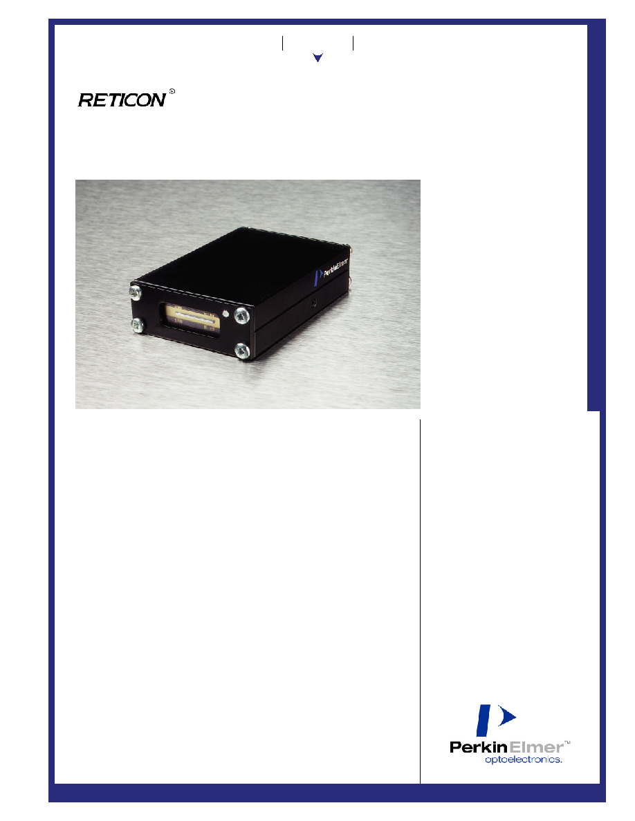
LC1917 Series Cameras
Low-Profile Analog Line Scan Camera
D
A
T
ASHEET
Lighting
Imaging
Telecom
Imaging Product Line
DSP-205.01A - 4/2001W Page 1
Description
In the LC1917 analog line scan camera,
PerkinElmer has combined the best
features of photodiode array detection,
high-speed charge-coupled scanning,
and analog line scan camera
technology to offer an uncompromising
solution to the increasing demands of
advanced imaging applications.
The LC1917 is a low profile analog line
scan camera. The LC1917 features a
single channel differential analog video
output format, with a resolution of
1024 pixels, which can achieve data
rates of up to 5 MHz with exceptional
noise immunity. It is designed for
volume applications where a small
profile is required.
One feature of typical line scan
cameras is a square profile face. While
this shape is unavoidable for area scan
cameras, it does not take advantage of
the long, thin active area of linear arrays.
The LC1917's flat faceplate measures
0.75" high by 2" wide. This size allows
the user to install multiple LC1917s
into an area scarcely big enough for
even the smallest square front profile
line scan camera.
The LC1917 converts light imaged
during a scene into an analog video
signal. The amplitude of the video sig-
nal is a linear function of the incident
illumination taken from the scene.
Antiblooming structures within the
sensor ensure superior performance
over a wide range of lighting condi-
tions. User-defined control is possible
for line rate, integration time and
video data rate.
LC1917 cameras may be interfaced to
most frame grabber cards, allowing for a
tested, plug and play solution. Typical
high performance line scan applications
include position monitoring, edge and
spot tracking, and acquisition of any
image generated by shadows, light
beams, or external optics.
Features
�
5 MHz output rate
�
Geometrically precise 14 �m square
pixel CCD
�
Small size: 0.75"H x 2"W x 3.077"L
�
High dynamic range (2500:1)
�
Antiblooming control
�
CE Mark
�
Adjustable gain and dark offset
levels
�
Line scan rates to 4.7 kHz
�
Differential digital I/O signals for
electrical noise immunity
0
150
250
350
450
550
650
750
850
950
1050
10
20
30
40
50
60
70
80
90
100
Wavelength (nm)
T
ransmission (%)
Analog Line Scan Cameras
www.perkinelmer.com/opto
DSP-205.01A - 4/2001W Page 2
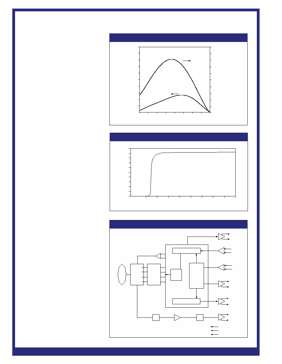
The Sensor
LC1917-series cameras contain a
high-performance, high-resolution line
scan image sensor (PerkinElmer
Optoelectronics parts RL1024PAG)
featuring a pinned photodiode pixel.
Each photodiode converts incident
light into discrete charge packets.
Advantages of pinned photodiode
pixels include linear exposure control,
the elimination of image lag, and the
reduction of photo response non-
uniformity (PRNU). For more specific
sensor specifications and information,
please consult the appropriate sensor
datasheet, available by contacting
PerkinElmer. Figure 1a details the
spectral sensitivity of the sensor,
while Figure 1b details the sensor's
glass window light transmission curve.
Functional Description
The video signal from the sensor is
processed through a single channel of
sampled-and-held, raster order, analog
video data. The video channel signal
processing circuitry offers both
adjustable gain and dark offset levels
to allow customization of the camera
to unique lighting applications. An
operational amplifier in a differential
configuration is recommended to
receive the video signal. Figure 2
details the camera video processing.
Input Signals
The LC1917 camera requires DC supply
voltages of +12 VDC, -12 VDC, and
+5 VDC for operation. Table 3 further
describes power requirements and
voltages, along with tolerances. By
default, the camera will operate at its
maximum line rate of 4700 scans per
second. The camera is controlled by
two externally generated differential
input signals: Master Clock (MCLK)
and Line Transfer (LT).
The Master Clock input determines
the data rate frequency for values up to
maximum clock of the camera (5 MHz).
The data rate may be run from 1 MHz
to cameras maximum clock rate.
The LT input signal transfers the
charge from each photosite to the
readout registers. The readout
registers, in turn, transport the charge
from each photodiode in succession to
the video outputs. The LT input from
the user must remain in the ON state
for at least one and a half MCLK
cycles to initiate the internal line
transfer and may remain ON until one
100
90
80
70
60
50
40
30
20
10
0
250
350
450
550
650
750
850
950
1050
100
90
80
70
60
50
40
30
20
10
0
Wavelength (nm)
Responsivity
(V/
�
J/cm
)
2
QE
(%)
Right Scale
Left Scale
Figure 1a. Spectral Sensitivity Curve (1X Gain)
Figure 1b. Sensor Window Transmission Curve
Figure 2. Camera Block Diagram
Line Transfer Logic
Line Enable Logic
FPGA
MCLK
Logic
Drive
Logic
LT
LEN
Level
T
rans
CLT+
CLT-
IMAGER
Buffer
Offset
ADJ
Gain
ADJ
Sample -
and - Hold
Amp
LENS
LEN+
LEN-
CCLK+
CCLK-
V
OUT+
V
OUT-
LT+
LT-
MCLK+
MCLK-
+12VDC
+5VDC
-12VDC
�
H
1
�
H
2
�
PG
�
RG
�
TG
�
AB
VIDEO
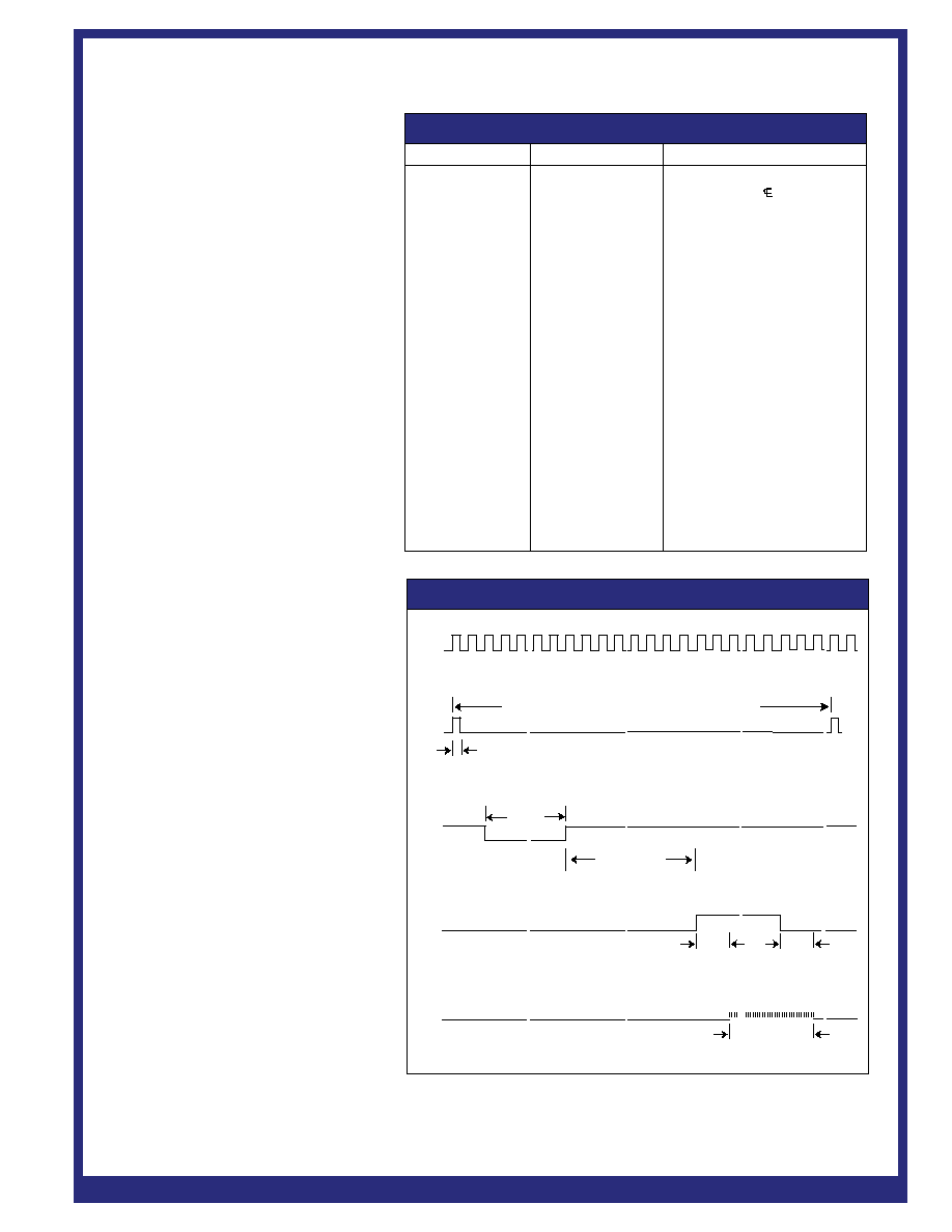
Table 2. Camera Description
Analog Line Scan Cameras
www.perkinelmer.com/opto
DSP-205.01A - 4/2001W Page 3
and a half clock cycles prior to the end
of read out. Because there are extra
stages in the CCD sensors readout regis-
ter, a minimum number of MCLK
cycles (the number of elements on the
CCD sensor plus 41) must exist
between successive LT commands.
The maximum line-scan period is 20
milliseconds. Integration times longer
than 20 ms can introduce higher levels
of dark current, which reduces the
dynamic range of the sensor. Longer
integration times are possible, however,
if the camera is cooled, which reduces
dark current. Specific application char-
acteristics, such as light level and rate
of object motion, will determine the
optimum setting. Timing details are
shown in Figure 3.
Output Signals
The LC1917-series camera provides
three output synchronization signals:
Camera Clock (CCLK), Line Enable
(LEN), and Camera Line Transfer (CLT).
The Camera Clock (CCLK) operates at
the MCLK frequency and is synchro-
nized to the analog video. The output
of the CCLK signal can be used to cap-
ture analog video data by a frame
grabber or digitizer.
The Line Enable (LEN) signal brackets
the valid analog video. The signal
becomes high two CCLK periods before
the first valid pixel and goes low two
CCLK periods before the last valid
pixel. The video output is a contiguous
pixel data stream with a dynamic
range (defined as peak video divided
by rms pixel noise) of greater than 2500:1.
The Camera Line Transfer (CLT) output
signal is an internally generated sync
signal. Its falling edge indicates the
start of a line readout sequence. This
signal may be used for controlling
strobes, shutters or other accessories
of the users system.
Video Signals
The LC1917 camera features an
adjustable DC offset. This offset is con-
trolled by a potentiometer, located
underneath the set screw on the body
side of the camera adjacent to active
Figure 3. Camera Timing Diagram
~~
~~
~~
~~
CCLK
LT
The minimum period between LT must be 41 + 1024 CLKS or 1065 clocks
LT minimum = 1.5 CLKS
CLT
CLT equals
6 CLKS
LEN
LEN leads and trails video by 2 CLKS
Video
1024 CLKS
CLT to LEN 11 CLKS
~~
~~
~~
~~
~~
~~
~~
~~
~~
~~
~~
~~
~~
~~
~~
~~
Parameter
Variable
Description
Physical
Optical Lens
No lens adaptor - optical
Sensor Alignment
Within �0.005" of of mounting hole
Dimensions
2" x 3.077" x 0.75"
Connector
Type
Amp C-216297
26-pin High Density Male
Cable Length
Maximum 10 meters
Power Requirements Operating Voltages
+12 VDC, +5 VDC, -12 VDC
Connection
Through 26-pin connector
Output
Data Rate
1 - 5 MHz
Type
Analog Differential Video
Connection
Through 26-pin connector
Control Signals
User Supplied
Master Clock (MCLK)
Line Transfer (LT)
User Communications
RS-422 Control Signals
Camera Supplied
Camera Clock (CCLK)
Line Enable (LEN)
Camera Line Transfer (CLT)
Connection
Through 26-pin connector
Sensor
Type
PerkinElmer RL1024PAG
Window
Glass
Operational
Gain Adjustment
5-Turn Potentiometer
Dark Offset Adjustment 5-Turn Potentiometer
Input Signals (contd.)
Analog Line Scan Cameras
www.perkinelmer.com/opto
Table 1. Pin Assignments
DSP-205.01A - 4/2001W Page 4
pixel 1024. This dark offset allows the
user to adjust the standard 0 V signal
�100 mV.
Additionally, the LC1917 camera
features a user-adjustable video gain,
allowing for video gains of up to 2.5X.
Video gain is adjustable using the
potentiometer, located underneath the
set screw on the body side adjacent to
the active pixel 1 side of the camera.
Both the gain and offset potentiometers
can also be adjusted by removing the
bottom plate of the camera. This is
accomplished by removing the two
lower screws on both the faceplate
and rear body of the camera. The cam-
era bottom is not attached to any
internal circuitry.
Proper ESD precautions should be
taken when removing the bottom plate
of the camera. Failure to do so can
result in camera failure.
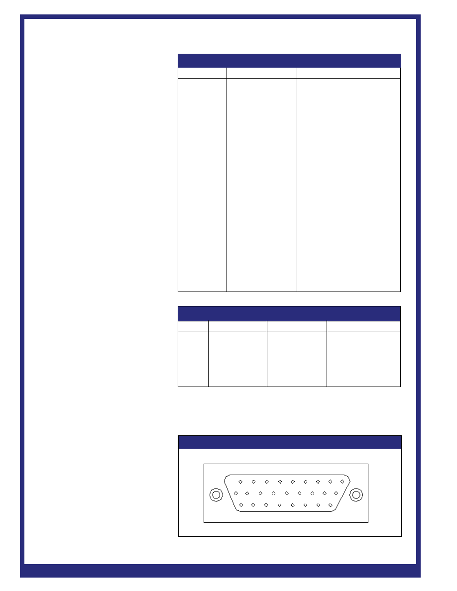
User Connections
The connector on the LC1917-series
camera is a 26-pin high density male
AMP C-216297. All user connections
are via this connector. It contains all
communications, output, and power
connections needed for camera opera-
tion. Refer to Table 1 for pinout locations
and details. Connector pin locations
are shown in Figure 4.
Optical Interface and Mounting
The LC1917 is to be mounted to the
user's optics via 4 M3 threaded screws,
located on the front panel of the
camera, adjacent to the sensor.
The optical surface of the sensor is
located 2.7mm (�10%) from the surface
face of the camera. The sensor has a
maximum angular error of �15
milliradians.
Camera Performance
The camera head is housed in a
rugged aluminum case, measuring
0.75"H x 2"W x 3.077"L (excluding
connector extensions) specifically
designed for close-proximity harsh
industrial applications. The sensor is
mounted on an aluminum plate that
efficiently transfers heat to the camera
case. The conductive cooling of this
surface is useful in minimizing ther-
mally generated dark current and
noise of the camera system.
Figure 4. Connector Diagram
1
2
3
4
5
6
7
8
9
10 11 12
13
14
15
16
17 18
19
20
21 22
23
24
25
26
Pin
Sym
Description
1
+12 VDC
12 VDC Input
2
+12 VDC
12 VDC Input
3
GND
Power Supply Ground
4
GND
Power Supply Ground
5
GND
Power Supply Ground
6
GND
Power Supply Ground
7
GND
Power Supply Ground
8
-12 VDC
-12 VDC Input
9
-12 VDC
-12 VDC Input
10
LT+
Line Transfer +
11
MCLK+
Master Clock +
12
CCLK+
Camera Clock +
13
LEN+
Line Enable +
14
CLT+
Camera Line Transfer +
15
+5VDC
5 VDC Input
16
GND
Power Supply Ground
17
GND
Power Supply Ground
18
VIDEO+
Video Out +
19
LT-
Line Transfer -
20
MCLK-
Master Clock -
21
CCLK-
Camera Clock -
22
LEN-
Line Enable -
23
CLT-
Camera Line Transfer -
24
+5 VDC
+5 VDC Input
25
GND
Power Supply Ground
26
VIDEO-
Video Out -
Table 3. Power Requirements
Pin
Voltage
Tolerance
Power Requirement
1
+12 VDC
�0.5 V
100 mA max
2
+12 VDC
�0.5 V
100 mA max
8
-12 VDC
�0.5 V
100 mA max
9
-12 VDC
�0.5 V
100 mA max
15
+5 VDC
�0.2 V
200 mA max
24
+5 VDC
�0.2 V
200 mA max
Notes
1. Cable length should not exceed 10 meters.
2. Noise and ripple <15mV p-p.
Video Signals (contd.)

Analog Line Scan Cameras
www.perkinelmer.com/opto
Table 4. Camera Specifications
DSP-205.01A - 4/2001W Page 5
Figure 5. Outline Drawings
2.00
(50.80)
0.75
(19.05)
3.077
(78.15)
FRONT VIEW
2.00
(50.80)
0.750
(19.05)
FACEPLATE VIEW
Pixel 1
Indicator
0.500
(12.70)
Sensor
0.375 (19.525)
1.772
(45.00)
� Sensor maximum angular error is
�
15 milliradians
� Optical surface of sensor is 2.7 mm (
�
10%) from
surface of camera
SIDE VIEW
M3 x 10 mm deep
3.077
(78.15)
MEASUREMENTS IN INCHES (MM)
0.750
(19.05)
Characteristic
Min
Typ
Max
Unit
Active Pixel Count
-
1024
-
elements
Pixel Size
-
14 x 14
-
�m
Pixel Spacing
-
14
-
�m
Spectral Response
250
-
1000
nm
Dynamic Range
4
-
2500:1
-
Ratio
Video Data Rate
1
-
5
MHz
Video Saturation Level
Typical (100 )
-
0.75
-
V
Differential (100 )
-
1.4
-
V
Gain Control
1
-
2.5
Factor
Dark Offset
-0.1
0
0.1
V
Saturation to FPN Dynamic Range
-
40
-
dB
Light Response Non-Uniformity
1, 2
-
�3
�6
%
Saturation Exposure
3
-
0.15
-
�J/cm
2
Photo Response Non-Uniformity
-
�10
-
%
Weight
-
-
20
ounces
Cable Length
-
-
10
meters
Operating Temperature
0
-
55
�Celsius
Storage Temperature
-40
-
80
�Celsius
Notes
1. 635 nm
2. At 50% light saturation
3. 500 nm
4. Dynamic Range = V
SAT
/rms noise.
O
O

www.perkinelmer.com/opto
For more information e-mail us at
opto@perkinelmer.com or visit our web
site at www.perkinelmer.com/opto.
All values are nominal; specifications
subject to change without notice.
� 2001 PerkinElmer Inc. All rights reserved.
PerkinElmer, the PerkinElmer logo and the stylized "P" are trademarks of PerkinElmer, Inc.
DSP-205.01A � 4/2001W
Reticon is a registered trademark of PerkinElmer, Inc.
Analog Line Scan Cameras
Page 6
Camera Model
Resolution
Max Data Rate
LC1917HAN-011
1024
5 MHz
Table 5. Stock Part Numbers
Table 6. Sales Offices
North America
United States
PerkinElmer Optoelectronics
2175 Mission College Blvd.
Santa Clara, CA 95054
Toll Free: 800-775-OPTO (6786)
Phone: +1-408-565-0830
Fax: +1-408-565-0703
Europe
Germany
PerkinElmer Optoelectronics GmbH
Wenzel-Jaksch-Str. 31
D-65199 Wiesbaden, Germany
Phone: +49-611-492-570
Fax: +49-611-492-165
Asia
Japan
PerkinElmer Optoelectronics
NEopt. 18F, Parale Mitsui Building 8
Higashida-Cho, Kawasaki-Ku
Kawasaki-Shi, Kanagawa-Ken 210-0005 Japan
Phone: +81-44-200-9170
Fax: +81-44-200-9160
www.neopt.co.jp
Singapore
47 Ayer Rajah Crescent #06-12
Singapore 139947
Phone: +65-770-4925
Fax: +65-777-1008
Ordering Information
While the information provided in
this data sheet is intended to describe
the form, fit and function for this
product, PerkinElmer reserves the
right to make changes without notice.