www.perkinelmer.com/opto
P-Series
Linear Photodiode Array Imagers
14µm, single output, 512, 1024, 2048 elements
Description
In the P-series linear imagers,
PerkinElmer has combined the best
features of high-sensitivity photodiode
array detection and high-speed charge-
coupled scanning to offer an uncom-
promising solution to the increasing
demands of advanced imaging
applications.
These high-performance imagers
feature low noise, high sensitivity,
impressive charge storage capacity,
and lag-free dynamic imaging in a
convenient single-output architecture.
The 14 µm square contiguous pixels in
these imagers reproduce images with
minimum information loss and artifact
generation, while their unique photo-
diode structure provides excellent blue
response extending below 250 nm in
the ultraviolet.
Features
∑
Extended spectral range--250 to
1000 nm
∑
40 MHz pixel readout rate
∑
2500:1 dynamic range
∑
5-volt clocking
∑
Line rates to 70 kHz
∑
Ultra low image lag
∑
Electronic exposure control
∑
Antiblooming control
∑
Square pixels with 100% fill factor
The two-phase CCD readout register
requires only five volts for clocking
yet achieves excellent charge transfer
efficiency. Additional electrodes
provide independent control of expo-
sure and antiblooming. Finally, the
high-sensitivity readout amplifier
provides a large output signal to relax
the noise requirements on the camera
electronics that follow.
Available in array lengths of 512, 1024
and 2048 elements with either low-
cost glass or UV-enhanced fused silica
windows, these versatile imagers are
widely used in high-speed document
reading, web inspection, mail sorting,
production measurement and gauging
position sensing, spectroscopy and
many other industrial and scientific
applications requiring peak imager
performance.
Note: While the P-Series imagers have been
designed to resist electrostatic discharge
(ESD), they can be damaged from such dis-
charges. Always observe proper ESD precau-
tions when handling and storing this imager.
D
A
T
ASHEET
Lighting
Imaging
Telecom
Imaging Product Line
DSP-101 01H - 7/2002W Page 1
Description (cont.)
P-series imagers combine high-perfor-
mance photodiodes with high-speed
CCD readout registers and a high-
sensitivity readout amplifier. Refer
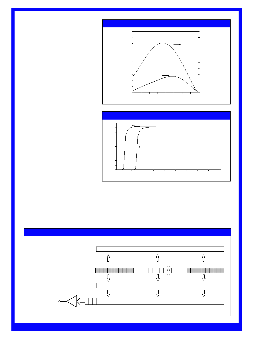
to Figure 1 for construction details.
Light Detection Area
The light detection area in P-series
imagers is a linear array of contiguous
pinned photodiodes on 14 µm centers.
These photodiodes are constructed
using PerkinElmer's advanced photo-
diode design that extends short-wave-
length sensitivity into the deep UV
below 250 nm, while preserving 100%
fill factor and delivering extremely
low image lag. This unique design
also avoids polysilicon layers in the
light detection area that reduces the
quantum efficiency of most CCD
imagers. The P-series imagers are sup-
plied with glass windows for general
visible use, and fused silica windows
for use in the ultraviolet below 350 nm.
See Figure 2 for the sensitivity and
window transmission curves.
For lowest lag, all P-series imagers
feature pinned photodiodes. Pinning,
which requires a special semiconduc-
tor process step, provides a uniform
internal voltage reference for the
charge stored in every photodiode.
This stable reference assures that
every photodiode is fully discharged
after every scan.
Figure 2a: Spectral Sensitivity Curve
100
90
80
70
60
50
40
30
20
10
0
250
350
450
550
650
750
850
950
1050
100
90
80
70
60
50
40
30
20
10
0
Wavelength (nm)
Responsivity
(V/
J
/cm
)
2
QE
(
%)
Right Scale
Left Scale
Figure 2b: Window Transmission Curve
Wavelength (nm)
T
r
ansmission (%)
100
90
80
70
60
50
40
30
20
10
0
150
450
350
250
550
950
850
750
650
1050
Fused Silica
Glass
Linear Photodiode Array
Imagers
www.perkinelmer.com/opto
Photodiodes covered with light
shields included at one or both ends
of the imager provide a dark current
reference for clamping. These are
separated from the active photodi-
odes by two unshielded transition
pixels that assure uniform response
out to the last active photodiode.
Due to the potential for light leak-
age, the two dark pixels nearest
the transition pixels should not
be used as a dark reference.
DSP-101 01H - 7/2002W Page 2
Figure 1: Imager Functional Diagram
{
Output
Amp
2-Phase Buried Channel CCD Shift Register
Transfer Gate
Antiblooming/Exposure Control Gate
D1 . . . . . . . . . . . . . . . . . . . .D10
T1 T2 1
2 3
. . . . . . . . .
D11 . . . . . . . . . . . . . . . . . . . .D20
N T3 T4
N-1
N = 512 for the RL0512P
N = 1024 for the RL1024P
N = 2048 for the RL2048P
3
Isolation stages
10
Dark pixels (D1 ... D10)
2
Transition pixels (T1, T2)
(Light shield ends between D10 and T1)
N
Active pixels (1...N)
2
Transition pixels (T3, T4)
(Light shield ends between T4 and D11)
10
Dark pixels (D11...D20) (Not used in RL0512P)
3 CCD Isolation Stages

Figure 4: Readout Timing Waveforms
ÿ
RG
t
1
t
2
t
6
t
4
t
5
ÿ
2
ÿ
1
Linear Photodiode Array
Imagers
www.perkinelmer.com/opto
Horizontal Shift Registers
Charge packets collected in the photo-
diodes as light is received are converted
to a serialized output stream through a
buried-channel, two-phase CCD shift
register that provides high charge trans-
fer efficiency at shift frequencies up to
40 MHz. The PerkinElmer 5-volt CCD
process used in this design enables
low-power, high-speed operation
with inexpensive, readily available
driver devices.
The transfer gate (ÿ
TG
) controls the
movement of charge packets from the
photodiodes to the CCD shift register.
During charge integration, the voltage
controlling the transfer gate is
held in its low state to isolate the
photodiodes from the shift register.
When transfer of charge to the shift
register is desired,
¯
TG
is switched to
its high state to create a transfer
channel between the photodiodes and
the shift register. The charge transfer
sequence, detailed in Figure 4, proceeds
as follows:
After readout of a particular image line
(n), the shift register is empty of charge
and ready to accept new charge packets
from the photodiodes representing
image line (n+1). To begin the transfer
sequence, the horizontal clock pulses
(
¯
1
and
¯
2
) are stopped with
¯
1
held in
its high state, and
¯
2
in its low state.
The transfer gate voltage phase (
¯
TG
) is
then switched high to start the transfer
of charge to the shift register. Once the
transfer gate reaches its high state, the
photo gate voltage (
¯
PG
) is set high to
complete the transfer. It is recom-
mended that the photo gate voltage be
held in the high state for at least 0.1 µs
to ensure complete transfer. After this
interval, the photo gate voltage is
returned to its low state, and when
that is completed, the transfer gate
voltage is also returned to the low
state. The details of the transfer timing
are shown in Figure 3 with ranges and
tolerances in Table 1.
After transfer, the charge is transported
along the shift register by the alternate
action of two horizontal phase voltages
DSP-101 01H - 7/2002W Page 3
Notes:
1. Transition and dark pixels
2. Active pixels
Figure 3: Transfer Timing Diagram
ÿ
TG
ÿ
1
V
Out
t
2
t
3
t
5
t
6
Note 1
Note 2
t
6
ÿ
PG
t
1
t
7
ÿ
AB
t
4
t
8
Item
Sym
Min
Typ
Max
Delay of
¯
TG
falling edge from
t
1
5 ns
20 ns
-
¯
PG
falling edge
Delay of
¯
TG
rising edge from end
of
¯
1
and
¯
2
clocks
t
2
0 ns
10 ns
-
Delay of
¯
AB
rising edge from
t
3
5 ns
5 ns
-
¯
PG
falling edge
¯
TG
pulse width
t
4
100 ns
500 ns
-
¯
PG
pulse width
t
5
100 ns
400 ns
-
Rise/fall time
t
6
10 ns
20 ns
-
Integration time
t
7
0 ns
-
-
¯
AB
pulse width
t
8
750 ns
1
-
-
Table 1. Transfer Timing Requirements
Note 1: 750ns is the typical time to fully reset the photodiode.

¯
1
and
¯
2
. While the two-phase CCD
shift register architecture allows
relaxed timing tolerances over those
required in three- or four-phase designs,
optimum charge transfer efficiency
and lowest power dissipation is
obtained when the overlap of the two-
phase CCD clocks occurs around the
50% transition level. Additionally, the
phase difference between signals
¯
1
and
¯
2
should be maintained near
180∞ and the duty cycle of both signals
should be set near 50% to prevent loss
of full-well charge storage capacity
and charge transfer efficiency. Readout
timing details are shown in Figure 4
with ranges and tolerances in Table 2.
Timing Requirements
In high-speed applications, fast
waveform transitions allow maximum
settling time of the output signal.
However, it is generally advisable to
use the slowest rise and fall times
consistent with required video
performance because fast edges tend
to introduce more transition noise
into the video waveform. When the
highest speeds are required, careful
smoothing of the waveform transitions
may improve the balance between
speed and video quality.
Output Amplifier
Charge emerging from the last stage
of the shift register is converted to a
voltage signal by a charge integrator
and video amplifier. The integrator, a
capacitor created by a floating diffusion,
is initially set to a DC reference volt-
age (V
RD
), by setting the reset transistor
voltage (
¯
RG
) to its high state. To read
out the charge,
¯
RG
is pulsed low
turning the reset transistor off and
isolating the integrator from V
RD
. The
next time
¯
1
goes low, the charge
packet is transferred to the integrator
where it generates a voltage propor-
tional to the packet size. The reset
transistor voltage,
¯
RG
, must reach
its low state prior to the high-to-low
transition of
¯
1
. An apparent clipping
of the video signal will result if this
Item
Sym
Min
Typ
Max
¯
1
,
¯
2
clock period
t
1
25 ns
-
-
¯
1
,
¯
2
rise/fall time
t
2
-
5 ns
-
¯
RG
rise/fall time
t
4
-
5 ns
-
¯
RG
clock - high duration
t
5
5 ns
-
-
Delay of
¯
1
high - low
t
6
0 ns
-
-
transition from
¯
RG
low*
Table 2. Readout Timing Requirements
Pixel count
512 elements (RL0512P)
1024 elements (RL1024P)
2048 elements (RL2048P)
Pixel size
14 µm x 14 µm
Exposure control
yes
Horizontal clocking
2
ÿ
(5V clock amplitude)
Number of outputs
1
Dynamic range
1
2500:1
Readout noise (rms)
amplifier
25 electrons
reset transistor
55 electrons
total noise without CDS
60 electrons
Saturation exposure
2
24 nJ/cm
2
Noise equivalent exposure
2
9.6 pJ/cm
2
Amplifier sensitivity
4 µV/electrons
Saturation output voltage
600 mv
Saturation charge capacity
150,000 electrons
Charge transfer efficiency
0.99995
Peak responsivity
25V/µJ/cm
2
PRNU match across array
±10%
Dead pixels
0
Lag
< 1%
Spectral response range
250 nm - 1000 nm
Data rate (per output)
40 MHz
Table 3. Imager Performance (Typical)
Linear Photodiode Array
Imagers
www.perkinelmer.com/opto
Notes:
1. Defined as Q
sat
/rms noise (total).
2. For illumination at 750 nm.
Note: The cross over point for
¯
1
and
¯
2
clock transitions should occur within the 10 - 90% level of the clock amplitude.
Horizontal Shift Registers (cont.)
DSP-101 01H - 7/2002W Page 4

condition is not satisfied. Figure 4
details the clock waveform require-
ments and overlap tolerances.
The video amplifier buffers the signal
from the integrator for output from the
imager. Care must be taken to keep the
load on this amplifier within its ability
to drive highly reactive or low imped-
ance loads. The half power bandwidth
into an external load of 10 pF is
150 MHz. It is recommended that the
output video signal be buffered with a
wide bandwidth emitter follower or
other appropriate amplifier to provide
a large Z
IN
to the output amplifier.
Keep the external amplifier close to
the output pins to minimize stray
inductive and capacitive coupling of
the output signal that can harm
signal quality.
Exposure Control and
Antiblooming
An exposure control feature in the
P-series imagers supports variable
charge accumulation time in the photo-
diode. When the antiblooming gate
voltage (
¯
AB
) is set to its high state,
charge is drained from the pixel
storage gate to the exposure control
drain. During normal charge collection
in the photodiode,
¯
AB
is set to its low
state. Due to the timing requirements
of the exposure control mode, charge
is always accumulated at the end of
the period just before the charge is
transferred to the readout register.
Figure 3 includes the timing require-
ments for exposure control with the
antiblooming gate. The exposure
control timing shown will act on the
charge packets that emerge as video
data on the next readout cycle.
Signal
Function
State
Voltage
Tolerance
¯
1
,
¯
2
Horizontal Clocks
High
5
±5%
Low
0
¯
TG
Transfer Gate
High
8
±10%
Low
0
¯
PG
Photo Gate
High
8
±5%
Low
-4
¯
AB
Antiblooming Gate
High
4
±5%
Low
-4
V
OG
Output Gate
3
±5%
¯
RG
Reset Gate
High
8
±10%
Low
0
V
DD
Amplifier Voltage Supply
12
±5%
V
RD
Amplifier Reset Drain
9.5
±5%
V
RD
/LS
Amplifier Return / Light Shield
0
Table 4. Operating Voltages
Min
Max
Units
Tempera
emperature
ture
Storage
-25
+85
∞ C
Operating
-25
+55
∞ C
V olta
oltage
ge (with
(with respect
respect to
to GND)
GND)
Pins 3, 4, 17 - 19
-0.3
+18
V
Pins 2, 10, 20
-0.3
+18
V
Pins 1, 11
-0.3
+ 0
V
Pins 15, 16
-4.3
+18
V
Table 5. Absolute Maximum Rating
Above Which Useful Life May Be Impaired
Linear Photodiode Array
Imagers
www.perkinelmer.com/opto
Imager Performance
In P-series images each element per-
forms its own function admirably
while integrating smoothly with the
other elements on the team. The pho-
todiodes efficiently transform light
to charge, the readout registers accu-
rately transport the charge to the
amplifier, and the amplifier delivers
Output Amplifier (cont.)
a clean, robust signal for use in
image processing electronics. While
the actual performance of these
imagers depends strongly on the
details of the electronics and timing
the camera provides, their straight-
forward implementation require-
ments facilitate optimum designs.
Precautionary Note: The CCD output pin (Pin #2) must never be shorted to either V
SS
or V
DD
while power is
applied to the device. Catastrophic device failure will result!
DSP-101 01H - 7/2002W Page 5