1996 Apr 26
2
Philips Semiconductors
Product specification
Voltage regulator diodes
1N5225B to 1N5267B
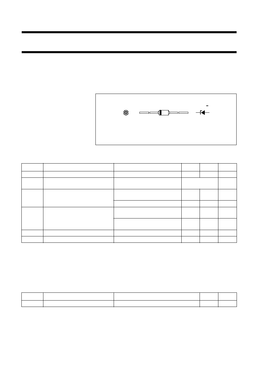
FEATURES
∑
Total power dissipation:
max. 500 mW
∑
Tolerance series:
±
5%
∑
Working voltage range:
nom. 3.0 to 75 V
∑
Non-repetitive peak reverse power
dissipation: max. 40 W.
APPLICATIONS
∑
Low-power voltage stabilizers or
voltage references.
DESCRIPTION
Low-power voltage regulator diodes in hermetically sealed leaded glass
SOD27 (DO-35) packages.
The series consists of 43 types with nominal working voltages from 3.0 to 75 V.
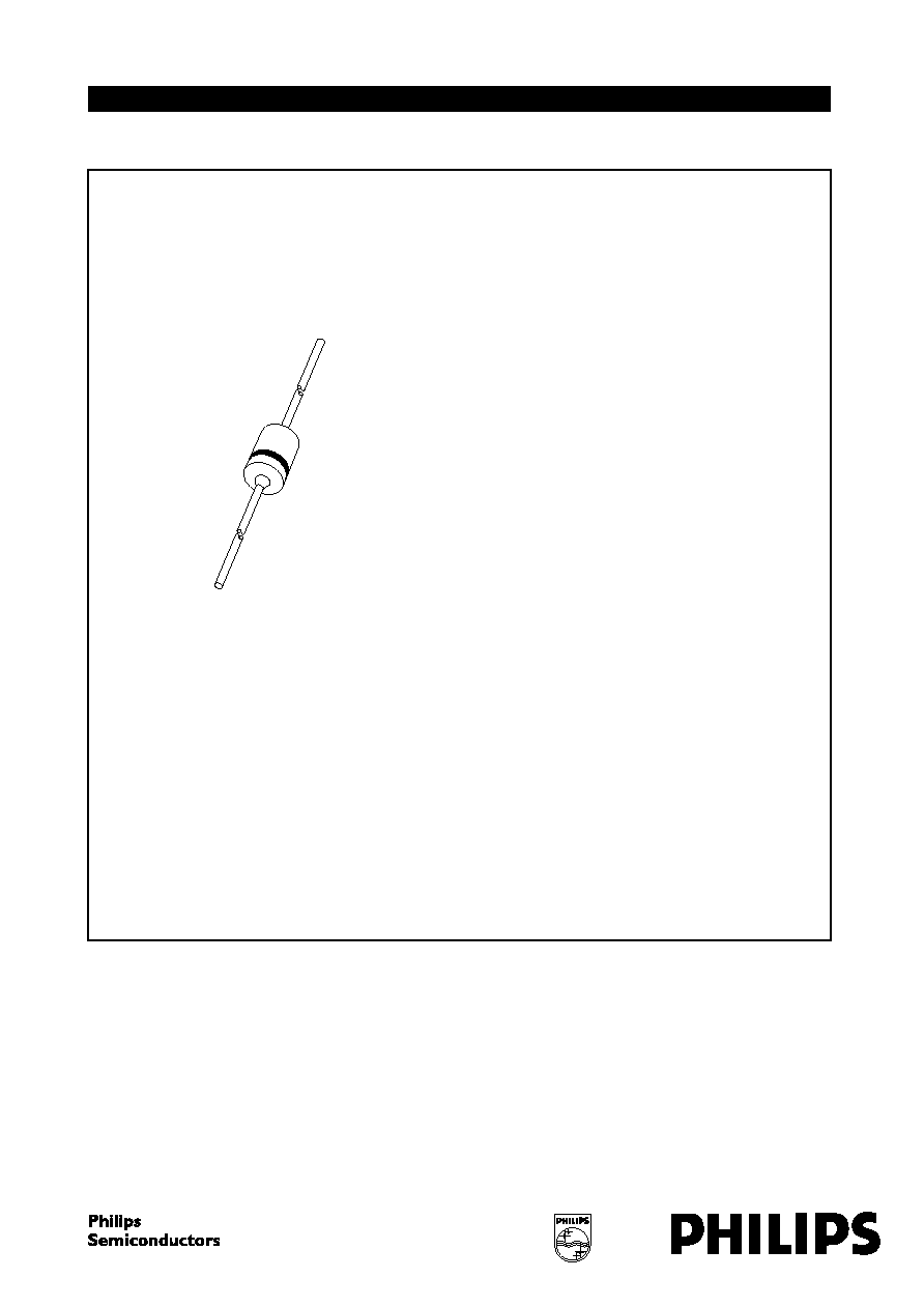
Fig.1 Simplified outline (SOD27; DO-35) and symbol.
The diodes are type branded.
handbook, halfpage
MAM239
k
a
LIMITING VALUES
In accordance with the Absolute Maximum Rating System (IEC 134).
Notes
1. Device mounted on a printed circuit-board without metallization pad.
2. Tie-point temperature
75
∞
C.
ELECTRICAL CHARACTERISTICS
Table 1
T
j
= 25
∞
C; unless otherwise specified.
SYMBOL
PARAMETER
CONDITIONS
MIN.
MAX.
UNIT
I
F
continuous forward current
-
250
mA
I
ZSM
non-repetitive peak reverse current
t
p
= 100
µ
s; square wave;
T
j
= 25
∞
C prior to surge
see Table
"Per type"
P
tot
total power dissipation
T
amb
= 50
∞
C; lead length max.;
note 1
-
400
mW
Lead length 8 mm; note 2
-
500
mW
P
ZSM
non-repetitive peak reverse power
dissipation
t
p
= 100
µ
s; square wave;
T
j
= 25
∞
C prior to surge; see Fig.3
-
40
W
t
p
= 8.3 ms; square wave;
T
j
55
∞
C prior to surge
-
10
W
T
stg
storage temperature
-
65
+200
∞
C
T
j
junction temperature
-
65
+200
∞
C
SYMBOL
PARAMETER
CONDITIONS
MAX.
UNIT
V
F
forward voltage
I
F
= 200 mA; see Fig.4
1.1
V
1996
Apr
26
4
Philips Semiconductors
Product specification
V
oltage regulator diodes
1N5225B to 1N5267B
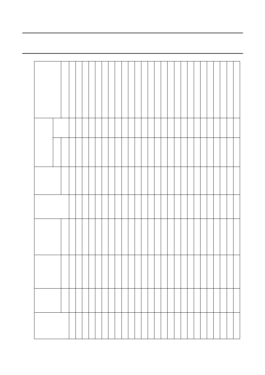
Notes
1. V
Z
is measured with device at thermal equilibrium while held in clips at 10 mm from body in still air at 25
∞
C.
2. For types 1N5225B to 1N5242B the I
Z
current is 7.5 mA; for 1N5243B and higher I
Z
= I
Ztest
. S
Z
values valid between 25
∞
C and 125
∞
C.
1N5251B
22
600
+0.087
5.6
60
0.1
17.0
1.25
1N5252B
24
600
+0.088
5.2
55
0.1
18.0
1.25
1N5253B
25
600
+0.089
5.0
55
0.1
19.0
1.25
1N5254B
27
600
+0.090
4.6
50
0.1
21.0
1.0
1N5255B
28
600
+0.091
4.5
50
0.1
21.0
1.0
1N5256B
30
600
+0.091
4.2
50
0.1
23.0
1.0
1N5257B
33
700
+0.092
3.8
45
0.1
25.0
0.9
1N5258B
36
700
+0.093
3.4
45
0.1
27.0
0.8
1N5259B
39
800
+0.094
3.2
45
0.1
30.0
0.7
1N5260B
43
900
+0.095
3.0
40
0.1
33.0
0.6
1N5261B
47
1000
+0.095
2.7
40
0.1
36.0
0.5
1N5262B
51
1100
+0.096
2.5
40
0.1
39.0
0.4
1N5263B
56
1300
+0.096
2.2
40
0.1
43.0
0.3
1N5264B
60
1400
+0.097
2.1
40
0.1
46.0
0.3
1N5265B
62
1400
+0.097
2.0
35
0.1
47.0
0.3
1N5266B
68
1600
+0.097
1.8
35
0.1
52.0
0.25
1N5267B
75
1700
+0.098
1.7
35
0.1
56.0
0.2
TYPE No.
WORKING
VOLTAGE
V
Z
(V)
(1)
at I
Ztest
DIFFERENTIAL
RESISTANCE
r
dif
(
)
at I
Ztest
TEMP. COEFF.
S
Z
(%/K)
at I
Z
(2)
TEST
CURRENT
I
Ztest
(mA)
DIODE CAP.
C
d
(pF)
at f = 1 MHz;
at V
R
= 0 V
REVERSE CURRENT
at REVERSE
VOLTAGE
NON-REPETITIVE PEAK
REVERSE CURRENT
I
ZSM
(A)
t
p
= 100
µ
s; T
amb
= 25
∞
C
I
R
(
µ
A)
V
R
(V)
NOM.
MAX.
MAX.
MAX.
MAX.
MAX.

1996 Apr 26
5
Philips Semiconductors
Product specification
Voltage regulator diodes
1N5225B to 1N5267B
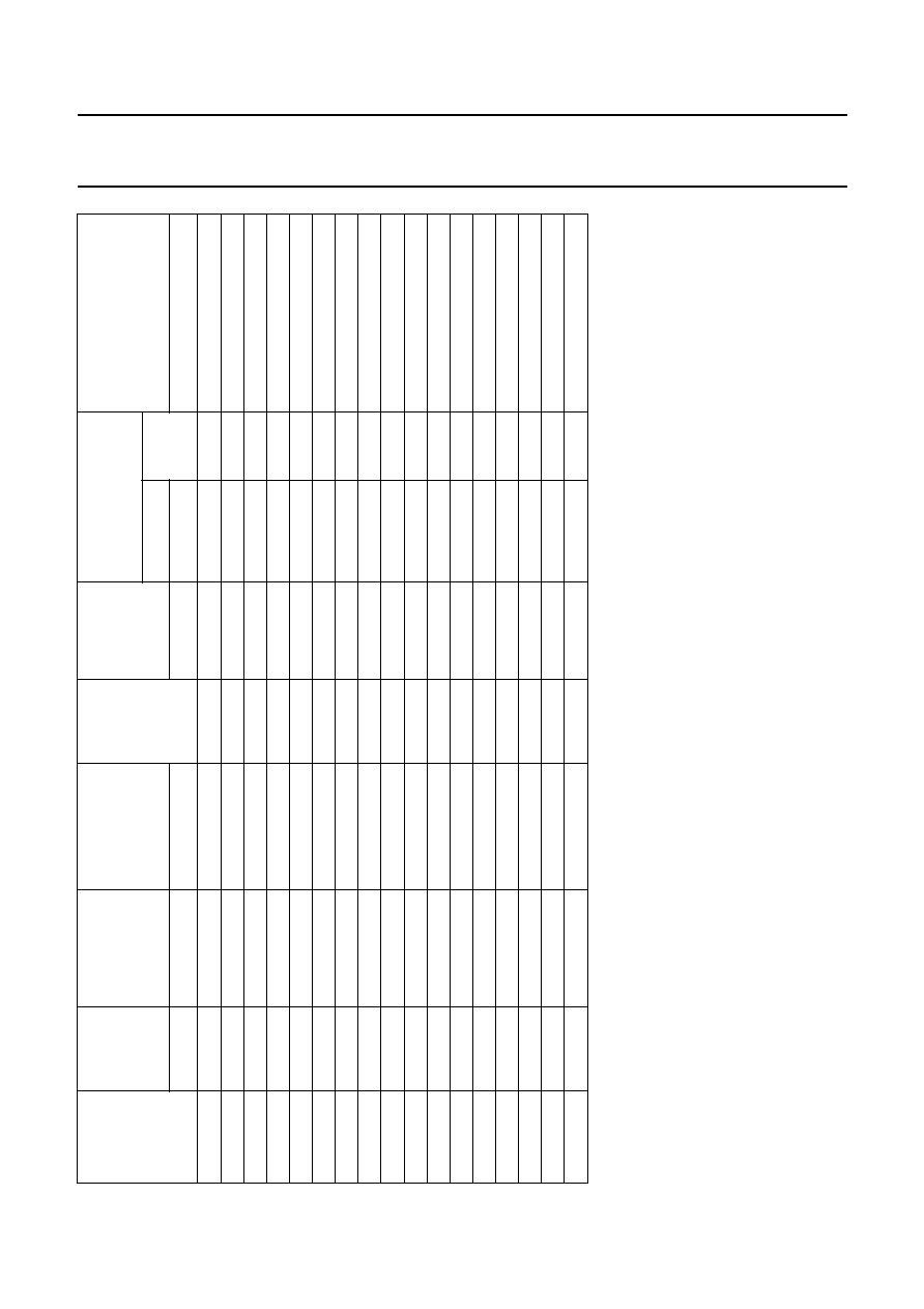
THERMAL CHARACTERISTICS
Note
1. Device mounted on a printed circuit-board without metallization pad.
SYMBOL
PARAMETER
CONDITIONS
VALUE
UNIT
R
th j-tp
thermal resistance from junction to tie-point lead length 10 mm
300
K/W
R
th j-a
thermal resistance from junction to ambient lead length max.; see Fig.2 and note 1
380
K/W