 | –≠–ª–µ–∫—Ç—Ä–æ–Ω–Ω—ã–π –∫–æ–º–ø–æ–Ω–µ–Ω—Ç: 2N2219 | –°–∫–∞—á–∞—Ç—å:  PDF PDF  ZIP ZIP |
Document Outline
- FEATURES
- APPLICATIONS
- DESCRIPTION
- PINNING
- QUICK REFERENCE DATA
- LIMITING VALUES
- THERMAL CHARACTERISTICS
- CHARACTERISTICS
- PACKAGE OUTLINE
- DEFINITIONS
- LIFE SUPPORT APPLICATIONS

DATA SHEET
Product specification
Supersedes data of 1997 May 07
File under Discrete Semiconductors, SC04
1997 Sep 03
DISCRETE SEMICONDUCTORS
2N2219; 2N2219A
NPN switching transistors
book, halfpage
M3D111
1997 Sep 03
2
Philips Semiconductors
Product specification
NPN switching transistors
2N2219; 2N2219A
FEATURES
∑
High current (max. 800 mA)
∑
Low voltage (max. 40 V).
APPLICATIONS
∑
High-speed switching
∑
DC and VHF/UHF amplification, for 2N2219 only.
DESCRIPTION
NPN switching transistor in a TO-39 metal package.
PNP complement: 2N2905 and 2N2905A.
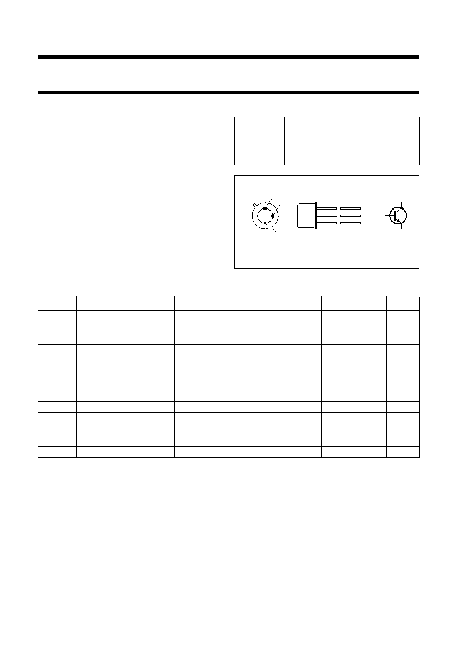
PINNING
PIN
DESCRIPTION
1
emitter
2
base
3
collector, connected to case
Fig.1 Simplified outline (TO-39) and symbol.
handbook, halfpage
3
1
2
MAM317
1
2
3
QUICK REFERENCE DATA
SYMBOL
PARAMETER
CONDITIONS
MIN.
MAX.
UNIT
V
CBO
collector-base voltage
open emitter
2N2219
-
60
V
2N2219A
-
75
V
V
CEO
collector-emitter voltage
open base
2N2219
-
30
V
2N2219A
-
40
V
I
C
collector current (DC)
-
800
mA
P
tot
total power dissipation
T
amb
25
∞
C
-
800
mW
h
FE
DC current gain
I
C
= 10 mA; V
CE
= 10 V
75
-
f
T
transition frequency
I
C
= 20 mA; V
CE
= 20 V; f = 100 MHz
2N2219
250
-
MHz
2N2219A
300
-
MHz
t
off
turn-off time
I
Con
= 150 mA; I
Bon
= 15 mA; I
Boff
=
-
15 mA
-
250
ns

1997 Sep 03
3
Philips Semiconductors
Product specification
NPN switching transistors
2N2219; 2N2219A
LIMITING VALUES
In accordance with the Absolute Maximum Rating System (IEC 134).
THERMAL CHARACTERISTICS
SYMBOL
PARAMETER
CONDITIONS
MIN.
MAX.
UNIT
V
CBO
collector-base voltage
open emitter
2N2219
-
60
V
2N2219A
-
75
V
V
CEO
collector-emitter voltage
2N2219
open base
-
30
V
2N2219A
open base; I
C
500 mA
-
40
V
V
EBO
emitter-base voltage
open collector
2N2219
-
5
V
2N2219A
-
6
V
I
C
collector current (DC)
-
800
mA
I
CM
peak collector current
-
800
mA
I
BM
peak base current
-
200
mA
P
tot
total power dissipation
T
amb
25
∞
C
-
800
mW
T
case
25
∞
C
-
3
W
T
stg
storage temperature
-
65
+150
∞
C
T
j
junction temperature
-
200
∞
C
T
amb
operating ambient temperature
-
65
+150
∞
C
SYMBOL
PARAMETER
CONDITIONS
VALUE
UNIT
R
th j-a
thermal resistance from junction to ambient
in free air
190
K/W
R
th j-c
thermal resistance from junction to case
50
K/W

1997 Sep 03
4
Philips Semiconductors
Product specification
NPN switching transistors
2N2219; 2N2219A
CHARACTERISTICS
T
j
= 25
∞
C unless otherwise specified.
SYMBOL
PARAMETER
CONDITIONS
MIN.
MAX.
UNIT
I
CBO
collector cut-off current
2N2219
I
E
= 0; V
CB
= 50 V
-
10
nA
I
E
= 0; V
CB
= 50 V; T
amb
= 150
∞
C
-
10
µ
A
I
CBO
collector cut-off current
2N2219A
I
E
= 0; V
CB
= 60 V
-
10
nA
I
E
= 0; V
CB
= 60 V; T
amb
= 150
∞
C
-
10
µ
A
I
EBO
emitter cut-off current
I
C
= 0; V
EB
= 3 V
-
10
nA
h
FE
DC current gain
I
C
= 0.1 mA; V
CE
= 10 V
35
-
h
FE
DC current gain
I
C
= 1 mA; V
CE
= 10 V
50
-
h
FE
DC current gain
I
C
= 10 mA; V
CE
= 10 V
75
-
h
FE
DC current gain
I
C
= 10 mA; V
CE
= 10 V; T
amb
=
-
55
∞
C
2N2219A
35
-
h
FE
DC current gain
I
C
= 150 mA; V
CE
= 1 V; note 1
50
-
h
FE
DC current gain
I
C
= 150 mA; V
CE
= 10 V; note 1
100
300
h
FE
DC current gain
I
C
= 500 mA; V
CE
= 10 V; note 1
2N2219
30
-
2N2219A
40
-
V
CEsat
collector-emitter saturation voltage
I
C
= 150 mA; I
B
= 15 mA; note 1
2N2219
-
400
mV
2N2219A
-
300
mV
V
CEsat
collector-emitter saturation voltage
I
C
= 500 mA; I
B
= 50 mA; note 1
2N2219
-
1.6
V
2N2219A
-
1
V
V
BEsat
base-emitter saturation voltage
I
C
= 150 mA; I
B
= 15 mA; note 1
2N2219
-
1.3
V
2N2219A
0.6
1.2
V
V
BEsat
base-emitter saturation voltage
I
C
= 500 mA; I
B
= 50 mA; note 1
2N2219
-
2.6
V
2N2219A
-
2
V
C
c
collector capacitance
I
E
= i
e
= 0; V
CB
= 10 V
-
8
pF
C
e
emitter capacitance
I
C
= i
c
= 0; V
EB
= 500 mV
2N2219A
-
25
pF
f
T
transition frequency
I
C
= 20 mA; V
CE
= 20 V; f = 100 MHz;
2N2219
250
-
MHz
2N2219A
300
-
MHz
F
noise figure
I
C
= 0.2 mA; V
CE
= 5 V; R
S
= 2 k
;
f = 1 kHz; B = 200 Hz
2N2219A
-
4
dB
1997 Sep 03
5
Philips Semiconductors
Product specification
NPN switching transistors
2N2219; 2N2219A
Note
1. Pulse test: t
p
300
µ
s;
0.02.
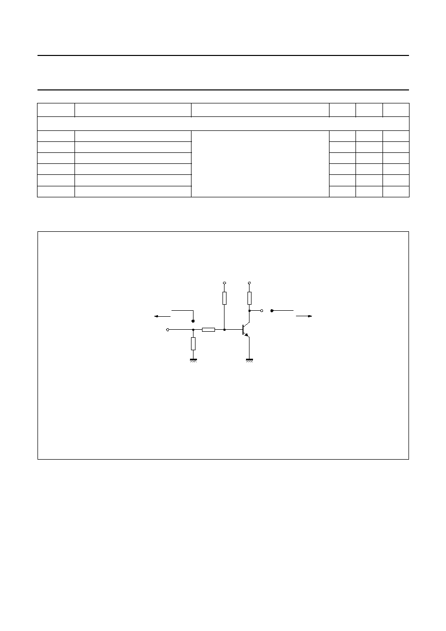
Switching times (between 10% and 90% levels) for type 2N2219A; see Fig.2
t
on
turn-on time
I
Con
= 150 mA; I
Bon
= 15 mA;
I
Boff
=
-
15 mA
-
35
ns
t
d
delay time
-
15
ns
t
r
rise time
-
20
ns
t
off
turn-off time
-
250
ns
t
s
storage time
-
200
ns
t
f
fall time
-
60
ns
SYMBOL
PARAMETER
CONDITIONS
MIN.
MAX.
UNIT
Fig.2 Test circuit for switching times.
handbook, full pagewidth
RC
R2
R1
DUT
MLB826
Vo
RB
(probe)
450
(probe)
450
oscilloscope
oscilloscope
VBB
Vi
VCC
V
i
= 9.5 V; T = 500
µ
s; t
p
=
10
µ
s; t
r
= t
f
3 ns.
R1 = 68
; R2 = 325
; R
B
= 325
; R
C
= 160
.
V
BB
=
-
3.5 V; V
CC
= 29.5 V.
Oscilloscope: input impedance Z
i
= 50
.