 | –≠–ª–µ–∫—Ç—Ä–æ–Ω–Ω—ã–π –∫–æ–º–ø–æ–Ω–µ–Ω—Ç: 2N2905A | –°–∫–∞—á–∞—Ç—å:  PDF PDF  ZIP ZIP |
Document Outline
- FEATURES
- APPLICATIONS
- DESCRIPTION
- PINNING
- QUICK REFERENCE DATA
- LIMITING VALUES
- THERMAL CHARACTERISTICS
- CHARACTERISTICS
- PACKAGE OUTLINE
- DEFINITIONS
- LIFE SUPPORT APPLICATIONS

DATA SHEET
Product specification
Supersedes data of September 1994
File under Discrete Semiconductors, SC04
1997 May 28
DISCRETE SEMICONDUCTORS
2N2905; 2N2905A
PNP switching transistors
book, halfpage
M3D111

1997 May 28
2
Philips Semiconductors
Product specification
PNP switching transistors
2N2905; 2N2905A
FEATURES
∑
High current (max. 600 mA)
∑
Low voltage (max. 60 V).
APPLICATIONS
∑
High-speed switching
∑
Driver applications for industrial service.
DESCRIPTION
PNP switching transistor in a TO-39 metal package.
NPN complements: 2N2219 and 2N2219A.
PINNING
PIN
DESCRIPTION
1
emitter
2
base
3
collector, connected to case
Fig.1
Simplified outline (TO-39) and symbol.
handbook, halfpage
3
1
2
MAM318
1
2
3
QUICK REFERENCE DATA
SYMBOL
PARAMETER
CONDITIONS
MIN.
MAX.
UNIT
V
CBO
collector-base voltage
open emitter
-
-
60
V
V
CEO
collector-emitter voltage
open base
2N2905
-
-
40
V
2N2905A
-
-
60
V
I
C
collector current (DC)
-
-
600
mA
P
tot
total power dissipation
T
amb
25
∞
C
-
600
mW
h
FE
DC current gain
I
C
=
-
150 mA; V
CE
=
-
10 V
100
300
f
T
transition frequency
I
C
=
-
50 mA; V
CE
=
-
20 V; f = 100 MHz
200
-
MHz
t
off
turn-off time
I
Con
=
-
150 mA; I
Bon
=
-
15 mA; I
Boff
= 15 mA
-
300
ns

1997 May 28
3
Philips Semiconductors
Product specification
PNP switching transistors
2N2905; 2N2905A
LIMITING VALUES
In accordance with the Absolute Maximum Rating System (IEC 134).
THERMAL CHARACTERISTICS
SYMBOL
PARAMETER
CONDITIONS
MIN.
MAX.
UNIT
V
CBO
collector-base voltage
open emitter
-
-
60
V
V
CEO
collector-emitter voltage
open base
2N2905
-
-
40
V
2N2905A
-
-
60
V
V
EBO
emitter-base voltage
open collector
-
-
5
V
I
C
collector current (DC)
-
-
600
mA
I
CM
peak collector current
-
-
800
mA
I
BM
peak base current
-
-
200
mA
P
tot
total power dissipation
T
amb
25
∞
C
-
600
mW
T
case
25
∞
C
-
3
W
T
stg
storage temperature
-
65
+150
∞
C
T
j
junction temperature
-
200
∞
C
T
amb
operating ambient temperature
-
65
+150
∞
C
SYMBOL
PARAMETER
CONDITIONS
VALUE
UNIT
R
th j-a
thermal resistance from junction to ambient
in free air
292
K/W
R
th j-c
thermal resistance from junction to case
58
K/W

1997 May 28
4
Philips Semiconductors
Product specification
PNP switching transistors
2N2905; 2N2905A
CHARACTERISTICS
T
amb
= 25
∞
C unless otherwise specified.
Note
1. Pulse test: t
p
300
µ
s;
0.02.
SYMBOL
PARAMETER
CONDITIONS
MIN.
MAX.
UNIT
I
CBO
collector cut-off current
2N2905
I
E
= 0; V
CB
=
-
50 V
-
-
20
nA
I
E
= 0; V
CB
=
-
50 V; T
amb
= 150
∞
C
-
-
20
µ
A
I
CBO
collector cut-off current
2N2905A
I
E
= 0; V
CB
=
-
50 V
-
-
10
nA
I
E
= 0; V
CB
=
-
50 V; T
amb
= 150
∞
C
-
-
10
µ
A
I
EBO
emitter cut-off current
I
C
= 0; V
EB
=
-
5 V
-
50
nA
h
FE
DC current gain
V
CE
=
-
10 V
2N2905
I
C
=
-
0.1 mA
35
-
I
C
=
-
1 mA
50
-
I
C
=
-
10 mA
75
-
I
C
=
-
150 mA; note 1
100
300
I
C
=
-
500 mA; note 1
30
-
h
FE
DC current gain
V
CE
=
-
10 V
2N2905A
I
C
=
-
0.1 mA
75
-
I
C
=
-
1 mA
100
-
I
C
=
-
10 mA
100
-
I
C
=
-
150 mA; note 1
100
300
I
C
=
-
500 mA; note 1
50
-
V
CEsat
collector-emitter saturation voltage I
C
=
-
150 mA; I
B
=
-
15 mA; note 1
-
-
400
mV
I
C
=
-
500 mA; I
B
=
-
50 mA; note 1
-
-
1.6
V
V
BEsat
base-emitter saturation voltage
I
C
=
-
150 mA; I
B
=
-
15 mA; note 1
-
-
1.3
V
I
C
=
-
500 mA; I
B
=
-
50 mA; note 1
-
-
2.6
V
C
c
collector capacitance
I
E
= i
e
= 0; V
CB
=
-
10 V; f = 1 MHz
-
8
pF
C
e
emitter capacitance
I
C
= i
c
= 0; V
EB
=
-
2 V; f = 1 MHz
-
30
pF
f
T
transition frequency
I
C
=
-
50 mA; V
CE
=
-
20 V; f = 100 MHz;
note 1
200
-
MHz
Switching times (between 10% and 90% levels); see Fig.2
t
on
turn-on time
I
Con
=
-
150 mA; I
Bon
=
-
15 mA; I
Boff
= 15 mA
-
45
ns
t
d
delay time
-
15
ns
t
r
rise time
-
35
ns
t
off
turn-off time
-
300
ns
t
s
storage time
-
250
ns
t
f
fall time
-
50
ns
1997 May 28
5
Philips Semiconductors
Product specification
PNP switching transistors
2N2905; 2N2905A
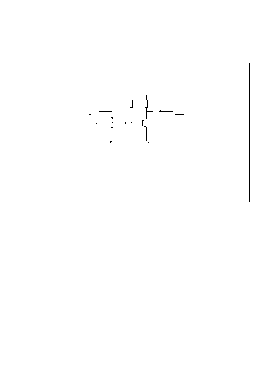
Fig.2 Test circuit for switching times.
ndbook, full pagewidth
RC
R2
R1
DUT
MGD624
Vo
RB
(probe)
450
(probe)
450
oscilloscope
oscilloscope
VBB
Vi
VCC
V
i
=
-
9.5 V; T = 500
µ
s; t
p
= 10
µ
s; t
r
= t
f
3 ns.
R1 = 68
; R2 = 325
µ
s; R
B
= 325
; R
C
= 160
.
V
BB
= 3.5 V; V
CC
=
-
29.5 V.
Oscilloscope input impedance Z
i
= 50
.