 | –≠–ª–µ–∫—Ç—Ä–æ–Ω–Ω—ã–π –∫–æ–º–ø–æ–Ω–µ–Ω—Ç: 2N3019 | –°–∫–∞—á–∞—Ç—å:  PDF PDF  ZIP ZIP |
Document Outline
- FEATURES
- APPLICATIONS
- DESCRIPTION
- PINNING
- QUICK REFERENCE DATA
- LIMITING VALUES
- THERMAL CHARACTERISTICS
- CHARACTERISTICS
- PACKAGE OUTLINE
- DEFINITIONS
- LIFE SUPPORT APPLICATIONS
DATA SHEET
Product specification
Supersedes data of September 1994
File under Discrete Semiconductors, SC04
1997 Jun 19
DISCRETE SEMICONDUCTORS
2N3019
NPN medium power transistor
book, halfpage
M3D111
1997 Jun 19
2
Philips Semiconductors
Product specification
NPN medium power transistor
2N3019
FEATURES
∑
High current (max. 1 A)
∑
Low voltage (max. 80 V).
APPLICATIONS
∑
Amplifier and switching circuits.
DESCRIPTION
NPN medium power transistor in a TO-39 metal package.
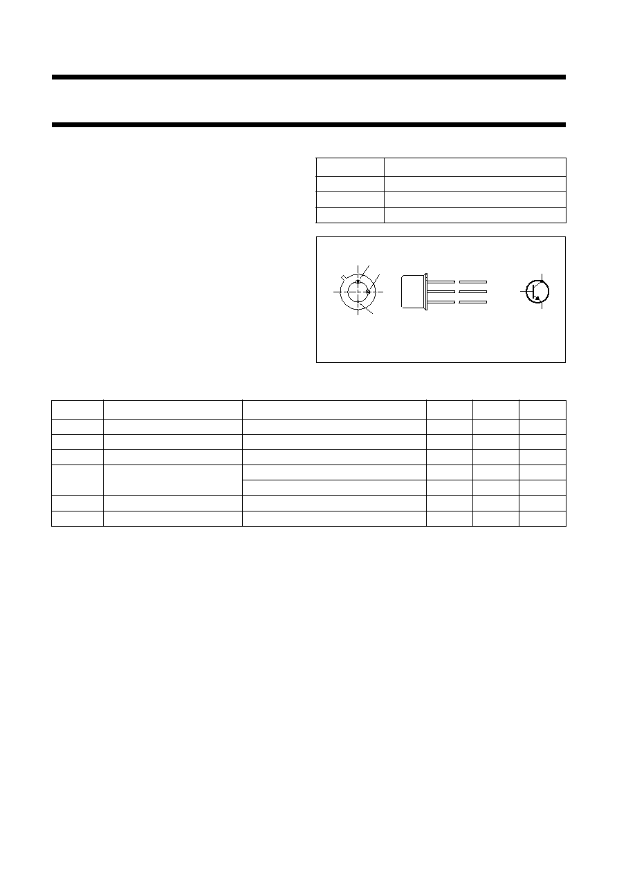
PINNING
PIN
DESCRIPTION
1
emitter
2
base
3
collector, connected to case
Fig.1 Simplified outline (TO-39) and symbol.
handbook, halfpage
3
1
2
MAM317
1
2
3
QUICK REFERENCE DATA
SYMBOL
PARAMETER
CONDITIONS
MIN.
MAX.
UNIT
V
CBO
collector-base voltage
open emitter
-
140
V
V
CEO
collector-emitter voltage
open base
-
80
V
I
C
collector current (DC)
-
1
A
P
tot
total power dissipation
T
amb
25
∞
C
-
800
mW
T
case
25
∞
C
-
5
W
h
FE
DC current gain
I
C
= 150 mA; V
CE
= 10 V
100
300
f
T
transition frequency
I
C
= 50 mA; V
CE
= 10 V; f = 100 MHz
100
-
MHz

1997 Jun 19
3
Philips Semiconductors
Product specification
NPN medium power transistor
2N3019
LIMITING VALUES
In accordance with the Absolute Maximum Rating System (IEC 134).
THERMAL CHARACTERISTICS
SYMBOL
PARAMETER
CONDITIONS
MIN.
MAX.
UNIT
V
CBO
collector-base voltage
open emitter
-
140
V
V
CEO
collector-emitter voltage
open base
-
80
V
V
EBO
emitter-base voltage
open collector
-
7
V
I
C
collector current (DC)
-
1
A
I
CM
peak collector current
-
1
A
I
BM
peak base current
-
200
mA
P
tot
total power dissipation
T
amb
25
∞
C
-
800
mW
T
case
25
∞
C
-
5
W
T
stg
storage temperature
-
65
+150
∞
C
T
j
junction temperature
-
200
∞
C
T
amb
operating ambient temperature
-
65
+150
∞
C
SYMBOL
PARAMETER
CONDITIONS
VALUE
UNIT
R
th j-a
thermal resistance from junction to ambient
in free air
218
K/W
R
th j-c
thermal resistance from junction to case
35
K/W

1997 Jun 19
4
Philips Semiconductors
Product specification
NPN medium power transistor
2N3019
CHARACTERISTICS
T
amb
= 25
∞
C unless otherwise specified.
Note
1. Pulse test: t
p
300
µ
s;
0.01.
SYMBOL
PARAMETER
CONDITIONS
MIN.
MAX.
UNIT
I
CBO
collector cut-off current
I
E
= 0; V
CB
= 90 V
-
10
nA
I
E
= 0; V
CB
= 90 V; T
amb
= 150
∞
C
-
10
µ
A
I
EBO
emitter cut-off current
I
C
= 0; V
EB
= 5 V
-
10
nA
h
FE
DC current gain
V
CE
= 10 V; note 1
I
C
= 0.1 mA
50
-
I
C
= 10 mA
90
-
I
C
= 150 mA
100
300
I
C
= 150 mA; T
case
=
-
55
∞
C
40
-
I
C
= 500 mA
50
-
I
C
= 1 A
15
-
V
CEsat
collector-emitter saturation voltage
I
C
= 150 mA; I
B
= 15 mA
-
200
mV
I
C
= 500 mA; I
B
= 50 mA; note 1
-
500
mV
V
BEsat
base-emitter saturation voltage
I
C
= 150 mA; I
B
= 15 mA; note 1
-
1.1
V
C
c
collector capacitance
I
E
= i
e
= 0; V
CB
= 10 V; f = 1 MHz
-
12
pF
C
e
emitter capacitance
I
C
= i
c
= 0; V
EB
= 500 mV; f = 1 MHz
-
60
pF
f
T
transition frequency
I
C
= 50 mA; V
CE
= 10 V; f = 20 MHz
100
-
MHz
F
noise figure
I
C
= 0.1 mA; V
CE
= 5 V; R
S
= 1 k
;
f = 1 kHz; B = 200 Hz
-
4
dB

1997 Jun 19
5
Philips Semiconductors
Product specification
NPN medium power transistor
2N3019
PACKAGE OUTLINE
UNIT
a
b
D
D
1
j
k
L
w
REFERENCES
OUTLINE
VERSION
EUROPEAN
PROJECTION
ISSUE DATE
IEC
JEDEC
EIAJ
mm
6.60
6.35
0.48
0.41
9.39
9.08
8.33
8.18
0.85
0.75
0.95
0.75
14.2
12.7
0.2
45
∞
DIMENSIONS (mm are the original dimensions)
SOT5/11
TO-39
97-04-11
k
j
D
A
L
seating plane
b
D
1
0
5
10 mm
scale
A
5.08
Metal-can cylindrical single-ended package; 3 leads
SOT5/11
A
w
A
M
M
B
M
B
a
1
2
3