DATA SHEET
Product specification
File under Integrated Circuits, IC04
January 1995
INTEGRATED CIRCUITS
HEF4027B
flip-flops
Dual JK flip-flop
For a complete data sheet, please also download:
∑
The IC04 LOCMOS HE4000B Logic
Family Specifications HEF, HEC
∑
The IC04 LOCMOS HE4000B Logic
Package Outlines/Information HEF, HEC

January 1995
2
Philips Semiconductors
Product specification
Dual JK flip-flop
HEF4027B
flip-flops
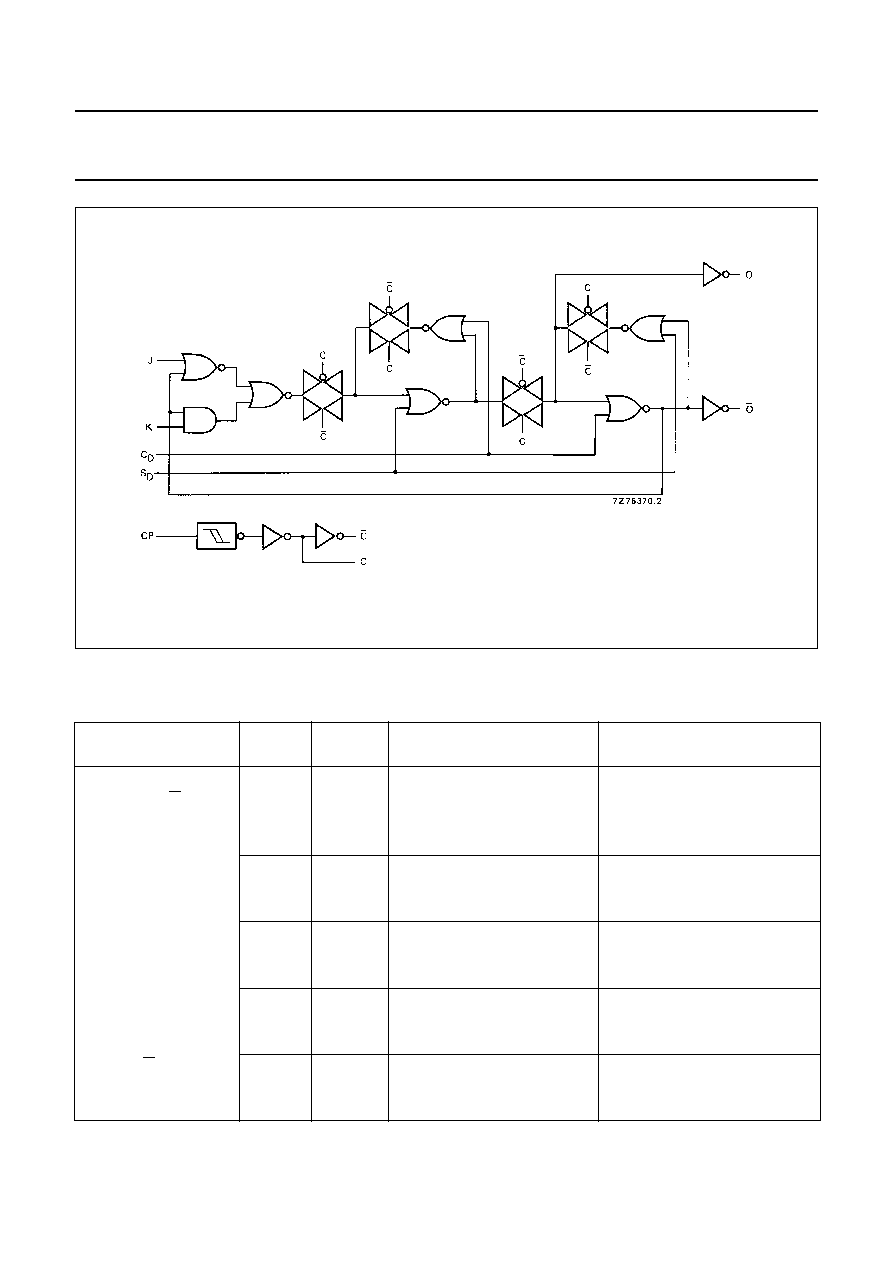
DESCRIPTION
The HEF4027B is a dual JK flip-flop which is
edge-triggered and features independent set direct
(S
D
), clear direct (C
D
), clock (CP) inputs and outputs
(O,O). Data is accepted when CP is LOW, and transferred
to the output on the positive-going edge of the clock. The
active HIGH asynchronous clear-direct (C
D
) and set-direct
(S
D
) are independent and override the J, K, and CP inputs.
The outputs are buffered for best system performance.
Schmitt-trigger action in the clock input makes the circuit
highly tolerant to slower clock rise and fall times.
Fig.1 Functional diagram.
Fig.2 Pinning diagram.
FUNCTION TABLES
Notes
1. H = HIGH state (the more positive voltage)
L = LOW state (the less positive voltage)
X = state is immaterial
= positive-going transition
O
n
+
1
= state after clock positive transition
PINNING
FAMILY DATA, I
DD
LIMITS category FLIP-FLOPS
See Family Specifications
INPUTS
OUTPUTS
S
D
C
D
CP
J
K
O
O
H
L
X
X
X
H
L
L
H
X
X
X
L
H
H
H
X
X
X
H
H
INPUTS
OUTPUTS
S
D
C
D
CP
J
K
O
n
+
1
O
n
+
1
L
L
L
L
no change
L
L
H
L
H
L
L
L
L
H
L
H
L
L
H
H
O
n
O
n
J,K
synchronous inputs
CP
clock input (L to H edge-triggered)
S
D
asynchronous set-direct input (active HIGH)
C
D
asynchronous clear-direct input (active HIGH)
O
true output
O
complement output
HEF4027BP(N):
16-lead DIL; plastic (SOT38-1)
HEF4027BD(F):
16-lead DIL; ceramic (cerdip) (SOT74)
HEF4027BT(D):
16-lead SO; plastic (SOT109-1)
( ): Package Designator North America

January 1995
5
Philips Semiconductors
Product specification
Dual JK flip-flop
HEF4027B
flip-flops
APPLICATION INFORMATION
Some examples of applications for the HEF4027B are:
∑
Registers
∑
Counters
∑
Control circuits
Fig.4
Waveforms showing set-up times, hold times and minimum clock pulse width. Set-up and hold times are
shown as positive values but may be specified as negative values.
Fig.5 Waveforms showing recovery times for S
D
and C
D
; minimum S
D
and C
D
pulse widths.