
DATA SHEET
Product specification
File under Integrated Circuits, IC04
January 1995
INTEGRATED CIRCUITS
HEF4042B
MSI
Quadruple D-latch
For a complete data sheet, please also download:
∑
The IC04 LOCMOS HE4000B Logic
Family Specifications HEF, HEC
∑
The IC04 LOCMOS HE4000B Logic
Package Outlines/Information HEF, HEC
January 1995
2
Philips Semiconductors
Product specification
Quadruple D-latch
HEF4042B
MSI
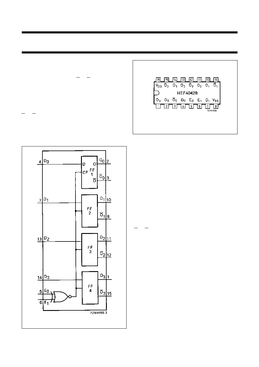
DESCRIPTION
The HEF4042B is a 4-bit latch with four data inputs (D
0
to
D
3
), four buffered latch outputs (O
0
to O
3
), four buffered
complementary latch outputs (O
0
to O
3
) and two common
enable inputs (E
0
and E
1
). Information on D
0
to D
3
is
transferred to O
0
to O
3
while both E
0
and E
1
are in the
same state, either HIGH or LOW. O
0
to O
3
follow D
0
to
D
3
as long as both E
0
and E
1
remain in the same state.
When E
0
and E
1
are different, D
0
to D
3
do not affect O
0
to
O
3
and the information in the latch is stored.
O
0
to O
3
are always the complement of O
0
to O
3
. The
exclusive-OR input structure allows the choice of either
polarity for E
0
and E
1
. With one enable input HIGH, the
other enable input is active HIGH; with one enable input
LOW, the other enable input is active LOW.
Fig.1 Functional diagram.
PINNING
APPLICATION INFORMATION
Some examples of applications for the HEF4042B are:
∑
Buffer storage
∑
Holding register
FAMILY DATA, I
DD
LIMITS category MSI
See Family Specifications
HEF4042BP(N):
16-lead DIL; plastic
(SOT38-1)
HEF4042BD(F):
16-lead DIL; ceramic (cerdip)
(SOT74)
HEF4042BT(D):
16-lead SO; plastic
(SOT109-1)
( ): Package Designator North America
D
0
to D
3
data inputs
E
0
and E
1
enable inputs
O
0
to O
3
parallel latch outputs
O
0
to O
3
complementary parallel latch outputs
Fig.2 Pinning diagram.

January 1995
3
Philips Semiconductors
Product specification
Quadruple D-latch
HEF4042B
MSI
Fig.3 Logic diagram.
Fig.4 Logic diagram (one latch).
FUNCTION TABLE
Note
1. H = HIGH state (the more positive voltage)
L = LOW state (the less positive voltage).
E
0
E
1
OUTPUT O
n
L
L
D
n
L
H
latched
H
L
latched
H
H
D
n
January 1995
4
Philips Semiconductors
Product specification
Quadruple D-latch
HEF4042B
MSI
AC CHARACTERISTICS
V
SS
= 0 V; T
amb
= 25
∞
C; C
L
= 50 pF; input transition times
20 ns
V
DD
V
SYMBOL
MIN.
TYP. MAX.
TYPICAL EXTRAPOLATION
FORMULA
Propagation delays
D
O, O
5
95
190
ns
67 ns
+
(0,55 ns/pF) C
L
HIGH to LOW
10
t
PHL
40
80
ns
28 ns
+
(0,23 ns/pF) C
L
15
30
55
ns
22 ns
+
(0,16 ns/pF) C
L
5
85
175
ns
57 ns
+
(0,55 ns/pF) C
L
LOW to HIGH
10
t
PLH
40
75
ns
28 ns
+
(0,23 ns/pF) C
L
15
30
60
ns
22 ns
+
(0,16 ns/pF) C
L
E
O, O
5
130
260
ns
102 ns
+
(0,55 ns/pF) C
L
HIGH to LOW
10
t
PHL
50
105
ns
38 ns
+
(0,23 ns/pF) C
L
15
35
75
ns
27 ns
+
(0,16 ns/pF) C
L
5
120
245
ns
92 ns
+
(0,55 ns/pF) C
L
LOW to HIGH
10
t
PLH
50
105
ns
38 ns
+
(0,23 ns/pF) C
L
15
35
75
ns
27 ns
+
(0,16 ns/pF) C
L
Output transition
times
5
60
120
ns
10 ns
+
(1,0 ns/pF) C
L
HIGH to LOW
10
t
THL
30
60
ns
9 ns
+
(0,42 ns/pF) C
L
15
20
40
ns
6 ns
+
(0,28 ns/pF) C
L
5
60
120
ns
10 ns
+
(1,0 ns/pF) C
L
LOW to HIGH
10
t
TLH
30
60
ns
9 ns
+
(0,42 ns/pF) C
L
15
20
40
ns
6 ns
+
(0,28 ns/pF) C
L
Set-up time
5
30
10
ns
see also waveforms
Figs 5 and 6
D
E
10
t
su
20
5
ns
15
20
5
ns
Hold time
5
15
-
5
ns
D
E
10
t
hold
15
0
ns
15
15
0
ns
Minimum enable
5
90
45
ns
pulse width
10
t
WE
40
20
ns
15
30
15
ns
V
DD
V
TYPICAL FORMULA FOR P (W)
Dynamic power
5
3800 f
i
+
(f
o
C
L
)
◊
V
DD
2
where
dissipation per
10
15 700 f
i
+
(f
o
C
L
)
◊
V
DD
2
f
i
= input freq. (MHz)
package (P)
15
41 100 f
i
+
(f
o
C
L
)
◊
V
DD
2
f
o
= output freq. (MHz)
C
L
= load capacitance (pF)
(f
o
C
L
) = sum of outputs
V
DD
= supply voltage (V)
January 1995
5
Philips Semiconductors
Product specification
Quadruple D-latch
HEF4042B
MSI
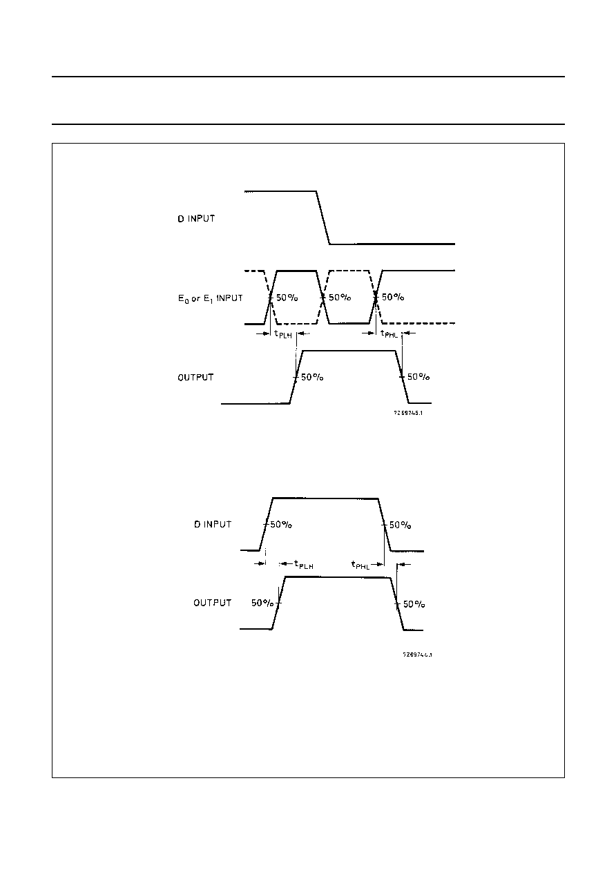
Fig.5 Waveforms showing propagation delays for D to O, with latch enabled.
Either E
0
or E
1
is held HIGH or LOW while the other enable input is pulsed as
the function table shows.