Philips
Semiconductors
74ABT16373B
74ABTH16373B
16-bit transparent latch (3-State)
Product specification
Supersedes data of 1995 Aug 03
IC23 Data Handbook
1998 Feb 27
INTEGRATED CIRCUITS
Philips Semiconductors
Product specification
74ABT16373B
74ABTH16373B
16-bit transparent latch (3-State)
2
1998 Feb 27
853-1751 19027
FEATURES
∑
16-bit transparent latch
∑
Multiple V
CC
and GND pins minimize switching noise
∑
Power-up 3-State
∑
Live insertion/extraction permitted
∑
Power-up reset
∑
3-State output buffers
∑
74ABTH16373B incorporates bus-hold data inputs which
eliminate the need for external pull-up resistors to hold unused
inputs
∑
Output capability: +64mA/≠32mA
∑
I
CCL
≠19 mA maximum
∑
Latch-up protection exceeds 500mA per JEDEC Std 17
∑
ESD protection exceeds 2000V per MIL STD 883 Method 3015
and 200V per Machine Model
DESCRIPTION
The 74ABT16373B high-performance BiCMOS device combines
low static and dynamic power dissipation with high speed and high
output drive.
The 74ABT16373B device is a dual octal transparent latch coupled
to two sets of eight 3-State output buffers. The two sections of the
device are controlled independently by Enable (nE) and Output
Enable (nOE) control gates.
The data on each set of D inputs are transferred to the latch outputs
when the Latch Enable (nE) input is High. The latch remains
transparent to the data inputs while nE is High, and stores the data
that is present one setup time before the High-to-Low enable
transition.
The 3-State output buffers are designed to drive heavily loaded
3-State buses, MOS memories, or MOS microprocessors. Each
active-Low Output Enable (nOE) controls eight 3-State buffers
independent of the latch operation.
When nOE is Low, the latched or transparent data appears at the
outputs. When nOE is High, the outputs are in the High-impedance
"OFF" state, which means they will neither drive nor load the bus.
Two options are available, 74ABT16373B which does not have the
bus-hold feature and 74ABTH16373B which incorporates the
bus-hold feature.
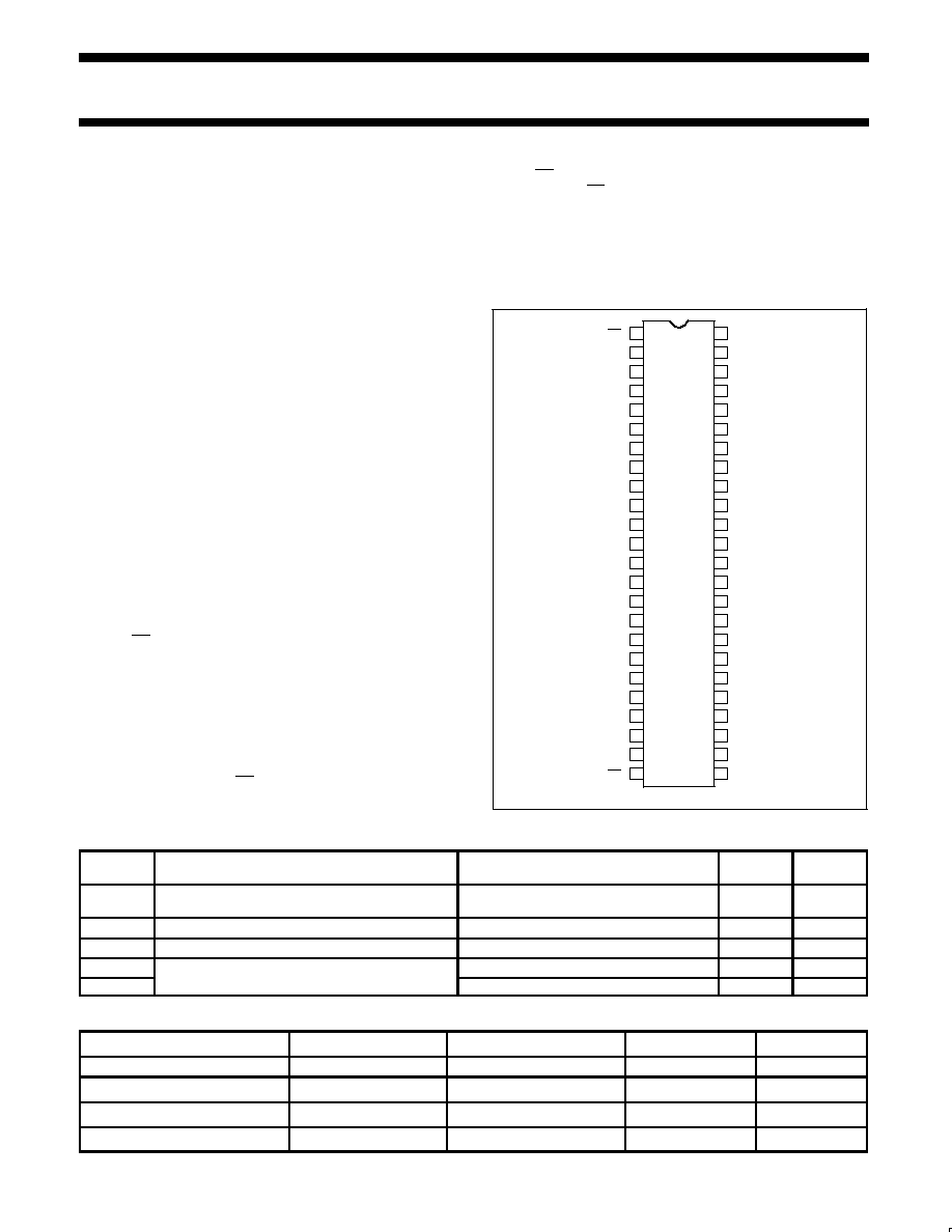
PIN CONFIGURATION
1
2
3
4
5
6
7
8
9
10
11
12
13
14
15
16
17
18
19
20
21
22
23
24
48
47
46
45
44
43
42
41
40
39
38
37
36
35
34
33
32
31
30
29
28
27
26
25
1OE
1Q0
1Q1
GND
1Q2
1Q3
1Q4
1Q5
GND
1Q6
1Q7
2Q0
2Q1
GND
2Q3
V
CC
2Q4
V
CC
2Q2
2Q5
GND
2Q7
2OE
2Q6
1E
1D0
1D1
GND
1D2
1D3
1D4
1D5
GND
1D6
1D7
2D0
2D1
GND
2D3
V
CC
2D4
V
CC
2D2
2D5
GND
2D7
2E
2D6
SA00379
QUICK REFERENCE DATA
SYMBOL
PARAMETER
CONDITIONS
T
amb
= 25
∞
C; GND = 0V
TYPICAL
UNIT
t
PLH
t
PHL
Propagation delay
Dn to Qn
C
L
= 50pF; V
CC
= 5V
2.5
2.0
ns
C
IN
Input capacitance
V
I
= 0V or V
CC
4
pF
C
OUT
Output capacitance
V
O
= 0V or V
CC
; 3-State
7
pF
I
CCZ
Quiescent supply current
Outputs disabled; V
CC
= 5.5V
500
µ
A
I
CCL
Quiescent su
ly current
Outputs low; V
CC
= 5.5V
8
mA
ORDERING INFORMATION
PACKAGES
TEMPERATURE RANGE
OUTSIDE NORTH AMERICA
NORTH AMERICA
DWG NUMBER
48-Pin SSOP type III
≠40
∞
C to +85
∞
C
74ABT16373B DL
BT16373B DL
SOT370-1
48-Pin TSSOP type II
≠40
∞
C to +85
∞
C
74ABT16373B DGG
BT16373B DGG
SOT362-1
48-Pin SSOP type III
≠40
∞
C to +85
∞
C
74ABTH16373B DL
BH16373B DL
SOT370-1
48-Pin TSSOP type II
≠40
∞
C to +85
∞
C
74ABTH16373B DGG
BH16373B DGG
SOT362-1
Philips Semiconductors
Product specification
74ABT16373B
74ABTH16373B
16-bit transparent latch (3-State)
1998 Feb 27
3
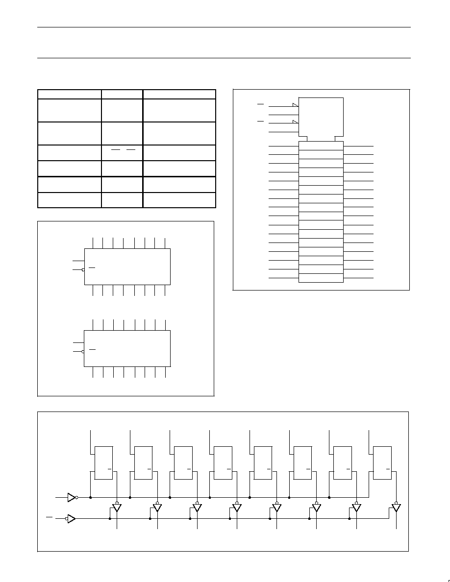
PIN DESCRIPTION
PIN NUMBER
SYMBOL
FUNCTION
47, 46, 44, 43, 41, 40,
38, 37, 36, 35, 33, 32,
30, 29, 27, 26
1D0 ≠ 1D7
2D0 ≠ 2D7
Data inputs
2, 3, 5, 6, 8, 9, 11, 12,
13, 14, 16, 17, 19, 20,
22, 23
1Q0 ≠ 1Q7
2Q0 ≠ 2Q7
Data outputs
1, 24
1OE, 2OE
Output enable inputs
(active-Low)
48, 25
1E, 2E
Enable inputs
(active-High)
4, 10, 15, 21, 28, 34,
39, 45
GND
Ground (0V)
7, 18, 31, 42
V
CC
Positive supply
voltage
LOGIC SYMBOL
3
2
1Q0 1Q1 1Q2
6
5
1Q3
47
46
44
43
1D0 1D1 1D2 1D3
48
1
9
8
1Q4 1Q5 1Q6
12
11
1Q7
41
40
38
37
1D4 1D5 1D6 1D7
1LE
1OE
14
13
17
16
36
35
33
32
25
24
20
19
23
22
30
29
27
26
2Q0 2Q1 2Q2 2Q3
2D0 2D21 2D2 2D3
2Q4 2Q5 2Q6 2Q7
2D4 2D5 2D6 2D7
2LE
2OE
SA00044
LOGIC SYMBOL (IEEE/IEC)
48
1EN
1
46
44
43
41
40
38
37
36
C3
2EN
C4
2
1
24
25
47
35
33
32
30
29
27
26
3
2
5
6
8
9
11
12
13
14
16
17
19
20
22
23
SA00380
1OE
1E
2OE
2E
1D0
1D1
1D2
1D3
1D4
1D5
1D6
2D0
2D1
2D2
2D3
2D4
2D5
2D6
2D7
1Q0
1Q1
1Q2
1Q3
1Q4
1Q5
1Q6
1Q7
2Q0
2Q1
2Q2
2Q3
2Q4
2Q7
1D7
2Q5
2Q6
3D
4D
LOGIC DIAGRAM
E
Q
D
nD0
nQ0
E
Q
D
nD1
E
Q
D
nD2
E
Q
D
nD3
E
Q
D
nD4
E
Q
D
nD5
E
Q
D
nD6
E
Q
D
nD7
nQ1
nQ2
nQ3
nQ4
nQ5
nQ6
nQ7
nLE
nOE
SA00046
Philips Semiconductors
Product specification
74ABT16373B
74ABTH16373B
16-bit transparent latch (3-State)
1998 Feb 27
4
FUNCTION TABLE
INPUTS
INTERNAL
OUTPUTS
OPERATING MODE
nOE
nE
nDx
REGISTER
nQ0 ≠ nQ7
OPERATING MODE
L
L
H
H
L
H
L
H
L
H
Enable and read register
L
L
i
h
L
H
L
H
Latch and read register
L
L
X
NC
NC
Hold
H
H
L
H
X
Dn
NC
Dn
Z
Z
Disable outputs
H = High voltage level
h
= High voltage level one set-up time prior to the High-to-Low E transition
L
= Low voltage level
l
= Low voltage level one set-up time prior to the High-to-Low E transition
NC= No change
X = Don't care
Z = High impedance "off" state
= High-to-Low E transition
ABSOLUTE MAXIMUM RATINGS
1, 2
SYMBOL
PARAMETER
CONDITIONS
RATING
UNIT
V
CC
DC supply voltage
≠0.5 to +7.0
V
I
IK
DC input diode current
V
I
< 0
≠18
mA
V
I
DC input voltage
3
≠1.2 to +7.0
V
I
OK
DC output diode current
V
O
< 0
≠50
mA
V
OUT
DC output voltage
3
output in Off or High state
≠0.5 to +5.5
V
I
O
DC output current
output in Low state
128
mA
I
OUT
DC output current
output in High state
≠64
mA
T
stg
Storage temperature range
≠65 to 150
∞
C
NOTES:
1. Stresses beyond those listed may cause permanent damage to the device. These are stress ratings only and functional operation of the
device at these or any other conditions beyond those indicated under "recommended operating conditions" is not implied. Exposure to
absolute-maximum-rated conditions for extended periods may affect device reliability.
2. The performance capability of a high-performance integrated circuit in conjunction with its thermal environment can create junction
temperatures which are detrimental to reliability. The maximum junction temperature of this integrated circuit should not exceed 150
∞
C.
3. The input and output voltage ratings may be exceeded if the input and output current ratings are observed.
RECOMMENDED OPERATING CONDITIONS
SYMBOL
PARAMETER
LIMITS
UNIT
SYMBOL
PARAMETER
MIN
MAX
UNIT
V
CC
DC supply voltage
4.5
5.5
V
V
I
Input voltage
0
V
CC
V
V
IH
High-level input voltage
2.0
V
V
IL
Low-level Input voltage
0.8
V
I
OH
High-level output current
≠32
mA
I
OL
Low-level output current
64
mA
t/
v
Input transition rise or fall rate
0
10
ns/V
T
amb
Operating free-air temperature range
≠40
+85
∞
C
Philips Semiconductors
Product specification
74ABT16373B
74ABTH16373B
16-bit transparent latch (3-State)
1998 Feb 27
5
DC ELECTRICAL CHARACTERISTICS
LIMITS
SYMBOL
PARAMETER
TEST CONDITIONS
T
amb
= +25
∞
C
T
amb
= ≠40
∞
C
to +85
∞
C
UNIT
MIN
TYP
MAX
MIN
MAX
V
IK
Input clamp voltage
V
CC
= 4.5V; I
IK
= ≠18mA
≠0.9
≠1.2
≠1.2
V
V
CC
= 4.5V; I
OH
= ≠3mA; V
I
= V
IL
or V
IH
2.5
2.9
2.5
V
V
OH
High-level output voltage
V
CC
= 5.0V; I
OH
= ≠3mA; V
I
= V
IL
or V
IH
3.0
3.4
3.0
V
V
CC
= 4.5V; I
OH
= ≠32mA; V
I
= V
IL
or V
IH
2.0
2.4
2.0
V
V
OL
Low-level output voltage
V
CC
= 4.5V; I
OL
= 64mA; V
I
= V
IL
or V
IH
0.42
0.55
0.55
V
V
RST
Power-up output voltage
3
V
CC
= 5.5V; I
O
= 1mA; V
I
= GND or V
CC
0.13
0.55
0.55
V
I
Input leakage current
V
CC
= 5 5V; V = V
CC
or GND
±
0 01
±
1
±
1
µ
A
I
I
g
74ABT16373B
V
CC
= 5.5V; V
I
= V
CC
or GND
±
0.01
±
1
±
1
µ
A
V
CC
= 5.5V; V
I
= V
CC
or GND
Control pins
±
0.01
±
1
±
1
µ
A
I
I
Input leakage current
74ABTH16373B
V
CC
= 5.5V; V
I
= V
CC
Data pins
5
0.01
1
1
µ
A
74ABTH16373B
V
CC
= 5.5V; V
I
= 0
Data pins
5
≠1
≠3
≠5
µ
A
6
V
CC
= 4.5V; V
I
= 0.8V
50
50
I
HOLD
Bus Hold current A inputs
6
74ABTH16373B
V
CC
= 4.5V; V
I
= 2.0V
≠75
≠75
µ
A
74ABTH16373B
V
CC
= 5.5V; V
I
= 0 to 5.5V
±
800
I
OFF
Power-off leakage current
V
CC
= 0.0V; V
O
or V
I
4.5V
±
5.0
±
100
±
100
µ
A
I
PU
/I
PD
Power-up/down 3-State
output current
4
V
CC
= 2.1V; V
O
= 0.5V; V
I
= GND or V
CC
;
V
OE
= GND
±
5.0
±
50
±
50
µ
A
I
OZH
3-State output High current
V
CC
= 5.5V; V
O
= 5.5V; V
I
= V
IL
or V
IH
0.5
10
10
µ
A
I
OZL
3-State output Low current
V
CC
= 5.5V; V
O
= 0.0V; V
I
= V
IL
or V
IH
≠0.5
≠10
≠10
µ
A
I
O
Output current
1
V
CC
= 5.5V; V
O
= 2.5V
≠50
≠70
≠180
≠50
≠180
mA
I
CEX
Output High leakage
current
V
CC
= 5.5V; V
O
= 5.5V; V
I
= GND or V
CC
0.1
50
50
µ
A
I
CCH
V
CC
= 5.5V; Outputs High, V
I
= GND or V
CC
0.5
2
2
mA
I
CCL
Quiescent supply current
V
CC
= 5.5V; Outputs Low, V
I
= GND or V
CC
8
19
19
mA
I
CCZ
V
CC
= 5.5V; Outputs 3-State;
V
I
= GND or V
CC
0.5
2
2
mA
I
CC
Additional supply current
per input pin
2
74ABT16373B
V
CC
= 5.5V; one input at 3.4V, other inputs
at V
CC
or GND
5
100
100
µ
A
I
CC
Additional supply current
per input pin
2
74ABTH16373B
V
CC
= 5.5V; one input at 3.4V, other inputs
at V
CC
or GND
0.5
1.5
1.5
mA
NOTES:
1. Not more than one output should be tested at a time, and the duration of the test should not exceed one second.
2. This is the increase in supply current for each input at 3.4V.
3. For valid test results, data must not be loaded into the flip-flops (or latches) after applying the power.
4. This parameter is valid for any V
CC
between 0V and 2.1V, with a transition time of up to 10msec. From V
CC
= 2.1 to V
CC
= 5V
±
10% a
transition time of up to 100
µ
sec is permitted.
5. Unused pins at V
CC
or GND.
6. This is the bus hold overdrive current required to force the input to the opposite logic state.