Philips Semiconductors
Product specification
74ABT16646
74ABTH16646
16-bit bus transceiver/register (3-State)
2
1998 Feb 27
853-1782 19026
FEATURES
∑
Independent registers for A and B buses
∑
Multiple V
CC
and GND pins minimize switching noise
∑
Live insertion/extraction permitted
∑
Power≠up 3-State
∑
Power≠up reset
∑
Multiplexed real-time and stored data
∑
Outputs sink 64mA and source 32mA
∑
Latch≠up protection exceeds 500mA per JEDEC Std 17
∑
74ABTH16646 incorporates bus-hold data inputs which eliminate
the need for external pull-up resistors to hold unused inputs
∑
ESD protection exceeds 2000V per MIL STD 883 Method 3015
and 200V per Machine Model
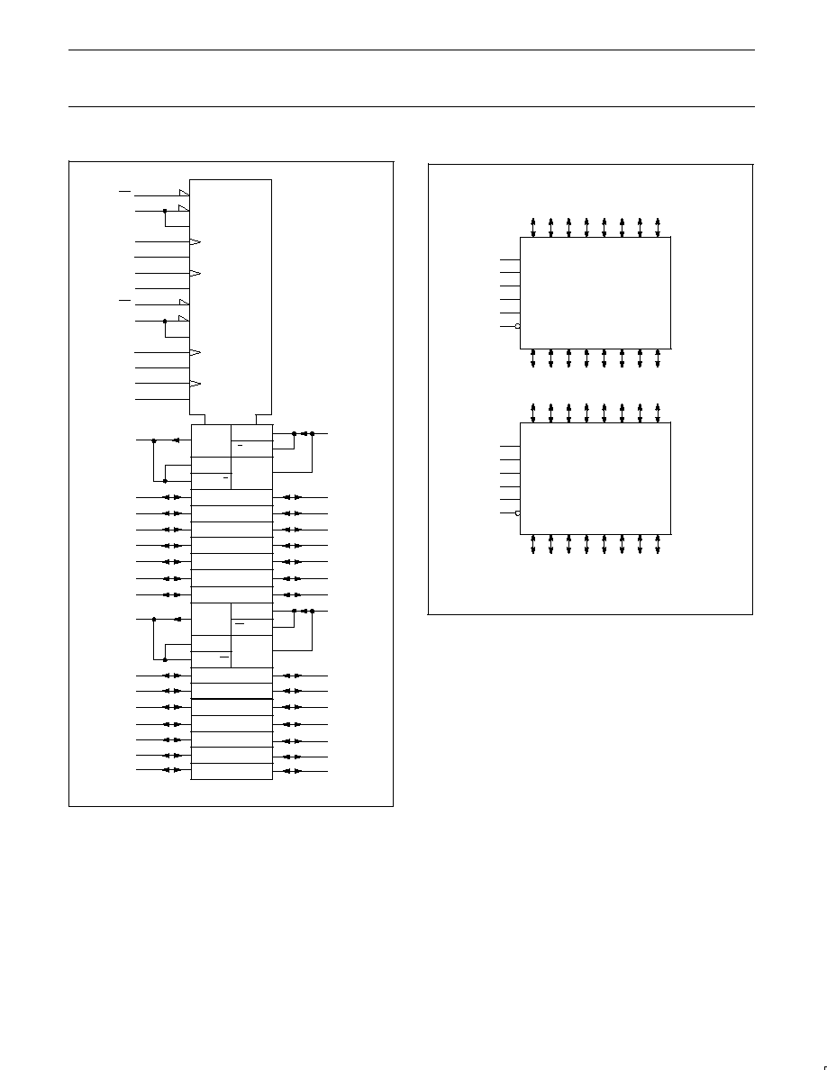
DESCRIPTION
The 74ABT16646 high≠performance BiCMOS device combines low
static and dynamic power dissipation with high speed and high
output drive.
The 74ABT16646 16-bit transceiver/register consists of two sets of
bus transceiver circuits with 3-State outputs, D-type flip-flops, and
control circuitry arranged for multiplexed transmission of data
directly from the input bus or from the internal registers. Data on the
A or B bus will be clocked into the registers as the appropriate clock
pin goes High. Output Enable (nOE) and Direction (nDIR) pins are
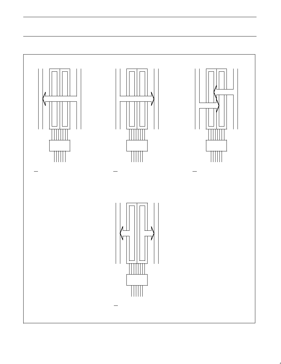
provided to control the transceiver function. In the transceiver mode,
data present at the high impedance port may be stored in either the
A or B register or both.
The select (nSAB, nSBA) pins determine whether data is stored or
transferred through the device in real-time. The nDIR determines
which bus will receive data when the nOE is active Low. In the
isolation mode (nOE = High), data from Bus A may be stored in the
B register and/or data from Bus B may be stored in the A register.
When an output function is disabled, the input function is still
enabled and may be used to store and transmit data. Only one of
the two buses, A or B may be driven at a time.
Two options are available, 74ABT16646 which does not have the
bus-hold feature and 74ABTH16646 which incorporates the
bus-hold feature.
QUICK REFERENCE DATA
SYMBOL
PARAMETER
CONDITIONS
T
amb
= 25
∞
C; GND = 0V
TYPICAL
UNIT
t
PLH
t
PHL
Propagation delay
nAx to nBx
C
L
= 50pF; V
CC
= 5V
3.3
2.7
ns
C
IN
Input capacitance
V
I
= 0V or V
CC
3
pF
C
I/O
I/O capacitance
V
O
= 0V or V
CC
; 3-State
7
pF
I
CC
Quiescent supply current
Outputs disabled; V
CC
=5.5V
550
µ
A
I
CCZ
Quiescent supply current
Outputs low; V
CC
=5.5V
9
mA
ORDERING INFORMATION
PACKAGES
TEMPERATURE RANGE
OUTSIDE NORTH AMERICA
NORTH AMERICA
DWG NUMBER
56-Pin Plastic SSOP Type III
≠40
∞
C to +85
∞
C
74ABT16646 DL
BT16646 DL
SOT371-1
56-Pin Plastic TSSOP Type II
≠40
∞
C to +85
∞
C
74ABT16646 DGG
BT16646 DGG
SOT364-1
56-Pin Plastic SSOP Type III
≠40
∞
C to +85
∞
C
74ABTH16646 DL
BH16646 DL
SOT371-1
56-Pin Plastic TSSOP Type II
≠40
∞
C to +85
∞
C
74ABTH16646 DGG
BH16646 DGG
SOT364-1
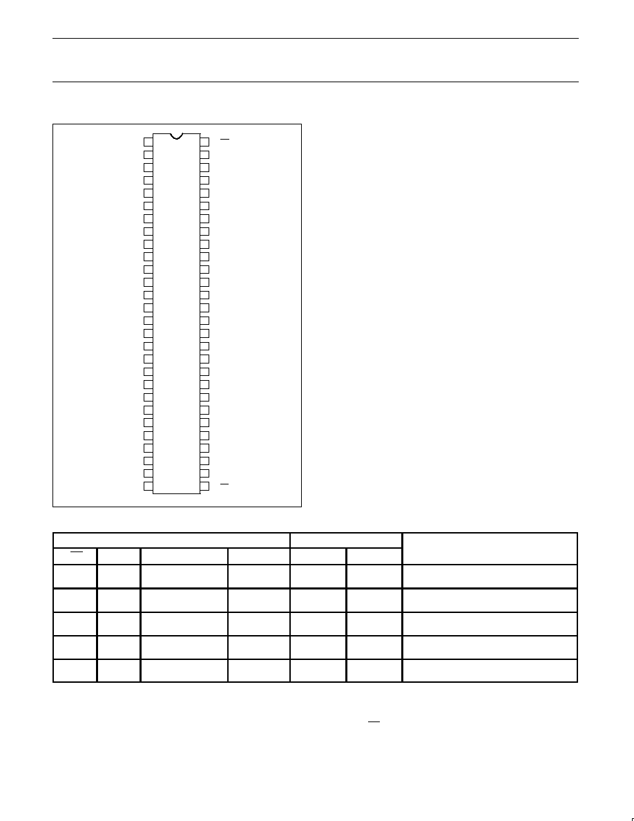
PIN DESCRIPTION
PIN NUMBER
SYMBOL
NAME AND FUNCTION
2, 55, 27, 30
1CPAB, 1CPBA, 2CPAB, 2CPBA
Clock input A to B / Clock input B to A
3, 54, 26, 31
1SAB, 1SBA, 2SAB, 2SBA
Select input A to B / Select input B to A
1, 28
1DIR, 2DIR
Direction control inputs
5, 6, 8, 9, 10, 12, 13, 14
15, 16, 17, 19, 20, 21, 23, 24
1A0 ≠ 1A7,
2A0 ≠ 2A7
Data inputs/outputs (A side)
52, 51, 49, 48, 47, 45, 44, 43
42, 41, 40, 38, 37, 36, 34, 33
1B0 ≠ 1B7,
2B0 ≠ 2B7
Data inputs/outputs (B side)
56, 29
1OE, 2OE
Output enable inputs
4, 11, 18, 25, 32, 39, 46, 53
GND
Ground (0V)
7, 22, 35, 50
V
CC
Positive supply voltage