1999 Sep 24
2
Philips Semiconductors
Product specification
Quad 2-input multiplexer
74AHC157;
74AHCT157
FEATURES
∑
ESD protection: HBM EIA/JESD22-A114-A
exceeds 2000 V MM EIA/JESD22-A115-A
exceeds 200 V CDM EIA/JESD22-C101
exceeds 1000 V
∑
Balanced propagation delays
∑
All inputs have Schmitt-trigger actions
∑
Multiple input enable for easy expansion
∑
Ideal for memory chip select decoding
∑
Inputs accept voltages higher than V
CC
∑
For AHC only: operates with CMOS input levels
∑
For AHCT only: operates with TTL input levels
∑
Specified from
-
40 to +85 and +125
∞
C.
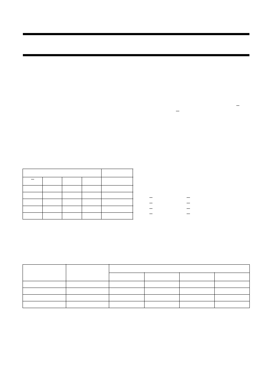
FUNCTION TABLE
See note 1.
Note
1. H = HIGH voltage level;
L = LOW voltage level;
X = don't care.
DESCRIPTION
The 74AHC/AHCT157 are high-speed Si-gate CMOS
devices and are pin compatible with low power Schottky
TTL (LSTTL). They are specified in compliance with
JEDEC standard No. 7A.
The 74AHC/AHCT157 are quad 2-input multiplexers which
select 4 bits of data from two sources under the control of
a common data select input (S). The enable input (E) is
active LOW. When E is HIGH, all of the outputs (1Y to 4Y)
are forced LOW regardless of all other input conditions.
Moving the data from two groups of registers to four
common output buses is a common use of the `157'. The
state of the common data select input (S) determines the
particular register from which the data comes. It can also
be used as a function generator.
The device is useful for implementing highly irregular logic
by generating any four of the 16 different functions of two
variables with one variable common.
The `157' is the logic implementation of a 4-pole, 2-position
switch, where the position of the switch is determine by the
logic levels applied to S.
The logic equations are:
1Y = E
◊
(1I
1
◊
S + 1I
0
◊
S);
2Y = E
◊
(2I
1
◊
S + 2I
0
◊
S);
3Y = E
◊
(3I
1
◊
S + 3I
0
◊
S);
4Y = E
◊
(4I
1
◊
S + 4I
0
◊
S).
The `157' is identical to the `158' but has non-inverting
(true) outputs.
INPUT
OUTPUT
E
S
nI
0
nI
1
nY
H
X
X
X
L
L
L
L
X
L
L
L
H
X
H
L
H
X
L
L
L
H
X
H
H
ORDERING INFORMATION
OUTSIDE NORTH
AMERICA
NORTH AMERICA
PACKAGES
PINS
PACKAGE
MATERIAL
CODE
74AHC157D
74AHC157D
16
SO
plastic
SOT109-1
74AHC157PW
74AHC157PW DH
16
TSSOP
plastic
SOT403-1
74AHCT157D
74AHCT157D
16
SO
plastic
SOT109-1
74AHCT157PW
74AHCT157PW DH
16
TSSOP
plastic
SOT403-1

1999 Sep 24
3
Philips Semiconductors
Product specification
Quad 2-input multiplexer
74AHC157;
74AHCT157
QUICK REFERENCE DATA
GND = 0 V; T
amb
= 25
∞
C; t
r
= t
f
3.0 ns.
Notes
1. C
PD
is used to determine the dynamic power dissipation (P
D
in
µ
W).
P
D
= C
PD
◊
V
CC
2
◊
f
i
+
(C
L
◊
V
CC
2
◊
f
o
) where:
f
i
= input frequency in MHz;
f
o
= output frequency in MHz;
(C
L
◊
V
CC
2
◊
f
o
) = sum of outputs;
C
L
= output load capacitance in pF;
V
CC
= supply voltage in Volts.
2. The condition is V
I
= GND to V
CC
.
PINNING
SYMBOL
PARAMETER
CONDITIONS
TYPICAL
UNIT
AHC
AHCT
t
PHL
/t
PLH
propagation delay
nI
0
, nI
1
to nY
C
L
= 15 pF; V
CC
= 5 V
3.2
3.4
ns
S to nY
C
L
= 15 pF; V
CC
= 5 V
4.5
5.1
ns
E to nY
C
L
= 15 pF; V
CC
= 5 V
3.7
4.0
ns
C
I
input capacitance
V
I
= V
CC
or GND
3.0
3.0
pF
C
O
output capacitance
4.0
4.0
pF
C
PD
power dissipation
capacitance
C
L
= 50 pF; f = 1 MHz; notes 1 and 2
4 outputs switching via S
31
41
pF
1 output switching via I
13
16
pF
PIN
SYMBOL
DESCRIPTION
1
S
common data select input
2, 5, 11 and 14
1I
0
to 4I
0
data inputs from source 0
3, 6, 10 and 13
1I
1
to 4I
1
data inputs from source 1
4, 7, 9 and 12
1Y to 4Y
multiplexer outputs
8
GND
ground (0 V)
15
E
enable input (active LOW)
16
V
CC
DC supply voltage


