2000 Aug 15
2
Philips Semiconductors
Product specification
8-bit serial-in/parallel-out shift register
74AHC164; 74AHCT164
FEATURES
∑
ESD protection:
HBM EIA/JESD22-A114-A exceeds 2000 V
MM EIA/JESD22-A115-A exceeds 200 V
CDM EIA/JESD22-C101 exceeds 1000 V
∑
Balanced propagation delays
∑
All inputs have Schmitt-trigger actions
∑
Inputs accept voltages higher than V
CC
∑
For AHC only: operates with CMOS input levels
∑
For AHCT only: operates with TTL input levels
∑
Specified from
-
40 to +85
∞
C and from
-
40 to +125
∞
C.
DESCRIPTION
The 74AHC/AHCT164 shift registers are high-speed
silicon-gate CMOS devices and are pin compatible with
Low power Schottky TTL (LSTTL). They are specified in
compliance with JEDEC standard No. 7A.
The 74AHC/AHCT164 input signals are 8-bit serial
through one of two inputs (D
sa
or D
sb
); either input can be
used as an active HIGH enable for data entry through the
other input. Both inputs must be connected together or an
unused input must be tied HIGH.
Data shifts one place to the right on each LOW-to-HIGH
transition of the clock (CP) input and enters into Q
0
, which
is a logical AND of the two data inputs (D
sa
, D
sb
) that
existed one set-up time prior to the rising clock edge.
A LOW level on the master reset (MR) input overrides all
other inputs and clears the register asynchronously,
forcing all outputs LOW.
QUICK REFERENCE DATA
GND = 0 V; T
amb
= 25
∞
C; t
r
= t
f
3.0 ns.
Notes
1. C
PD
is used to determine the dynamic power dissipation (P
D
in
µ
W).
P
D
= C
PD
◊
V
CC
2
◊
f
i
+
(C
L
◊
V
CC
2
◊
f
o
) where:
f
i
= input frequency in MHz;
f
o
= output frequency in MHz;
(C
L
◊
V
CC
2
◊
f
o
) = sum of outputs;
C
L
= output load capacitance in pF;
V
CC
= supply voltage in Volts.
2. The condition is V
I
= GND to V
CC
.
SYMBOL
PARAMETER
CONDITIONS
TYPICAL
UNIT
AHC
AHCT
t
PHL
/t
PLH
propagation delay
C
L
= 15 pF; V
CC
= 5 V
CP to Q
n
4.5
3.4
ns
MR to Q
n
4.0
3.5
ns
C
I
input capacitance
V
I
= V
CC
or GND
3
3
pF
f
max
maximum clock frequency
C
L
= 15 pF; V
CC
= 5 V
175
175
MHz
C
PD
power dissipation capacitance
C
L
= 50 pF; f = 1 MHz; notes 1 and 2
48
51
pF
2000 Aug 15
3
Philips Semiconductors
Product specification
8-bit serial-in/parallel-out shift register
74AHC164; 74AHCT164
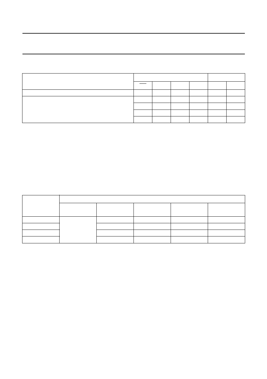
FUNCTION TABLE
See note 1.
Note
1. H = HIGH voltage level;
h = HIGH voltage level one set-up time prior to the LOW-to-HIGH clock transition;
L = LOW voltage level;
l = LOW voltage level one set-up time prior to the LOW-to-HIGH clock transition;
= LOW-to-HIGH transition;
X = don't care;
q = lower case letter indicates the state of the referenced input one set-up time prior to the LOW-to-HIGH transition.
ORDERING INFORMATION
OPERATING MODES
INPUTS
OUTPUTS
MR
CP
D
sa
D
sb
Q
0
Q
1
-Q
7
reset (clear)
L
X
X
X
L
L-L
shift
H
l
l
L
q
0
-q
6
H
l
h
L
q
0
-q
6
H
h
l
L
q
0
-q
6
H
h
h
H
q
0
-q
6
TYPE NUMBER
PACKAGES
TEMPERATURE
RANGE
PINS
PACKAGE
MATERIAL
CODE
74AHC164D
-
40 to +125
∞
C
14
SO
plastic
SOT108-1
74AHC164PW
14
TSSOP
plastic
SOT402-1
74AHCT164D
14
SO
plastic
SOT108-1
74AHCT164PW
14
TSSOP
plastic
SOT402-1

2000 Aug 15
4
Philips Semiconductors
Product specification
8-bit serial-in/parallel-out shift register
74AHC164; 74AHCT164
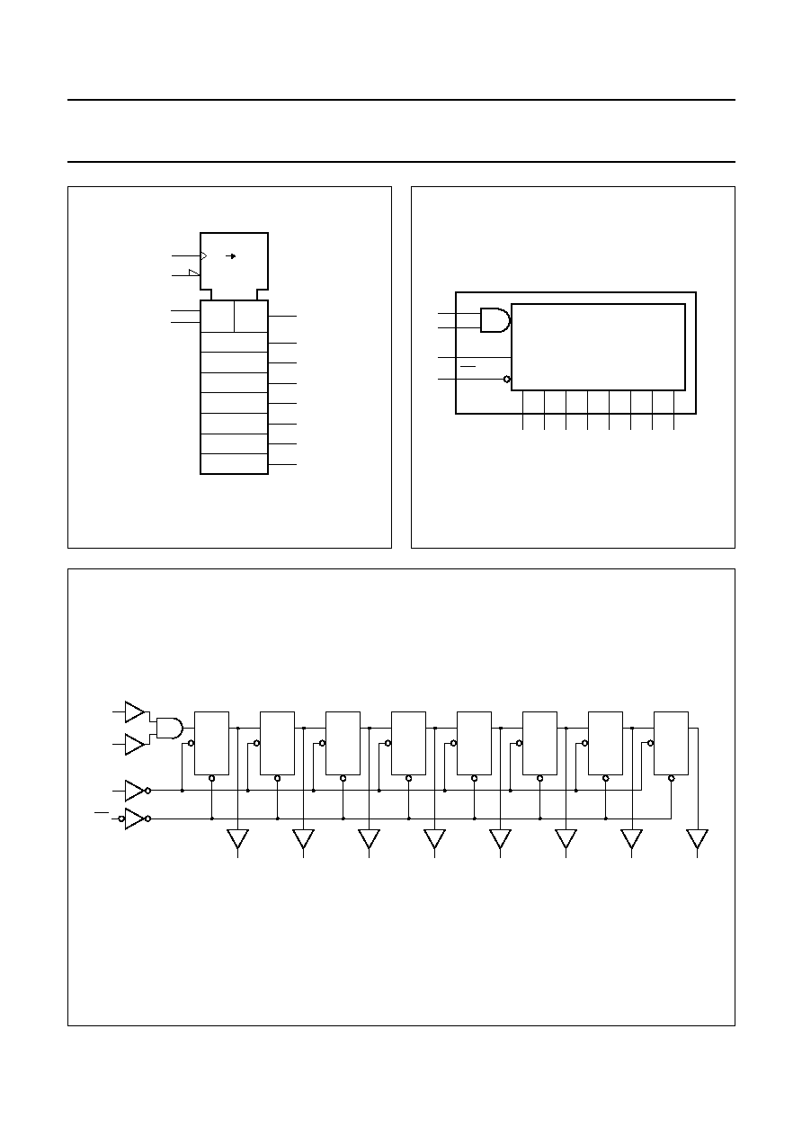
PINNING
PIN
SYMBOL
DESCRIPTION
1, 2
D
sa
, D
sb
data input
3, 4, 5, 6, 10, 11, 12, 13
Q
0
to Q
7
outputs
7
GND
ground (0 V)
8
CP
clock input (LOW-to-HIGH, edge-triggered)
9
MR
master reset input (active LOW)
14
V
CC
DC supply voltage
handbook, halfpage
164
MNA596
1
2
3
4
5
6
7
Dsa
Dsb
Q0
Q1
Q2
Q3
GND
VCC
Q7
Q6
Q5
Q4
MR
CP
14
13
12
11
10
9
8
Fig.1 Pin configuration.
handbook, halfpage
13
MNA597
Q7
Q6
Q5
Q4
Q3
Q2
Q1
Dsb
Dsa
Q0
12
MR
CP
11
10
6
5
4
3
1
2
8
9
Fig.2 Logic symbol.