
2003 Jul 21
2
Philips Semiconductors
Product specification
Octal D-type flip-flop with reset;
positive-edge trigger
74AHC273; 74AHCT273
FEATURES
∑
Ideal buffer for MOS microcontroller or memory
∑
Common clock and master reset
∑
ESD protection:
HBM EIA/JESD22-A114-A exceeds 2000 V
MM EIA/JESD22-A115-A exceeds 200 V.
∑
Balanced propagation delays
∑
All inputs have Schmitt-trigger actions
∑
Inputs accepts voltages higher than V
CC
∑
Related products:
≠ See 74AHC(T)377 for clock enable version
≠ See 74AHC(T)373 for transparent latch version
≠ See 74AHC(T)374 for 3-state version.
∑
For AHC only: operates with CMOS input levels
∑
For AHCT only: operates with TTL input levels
∑
Specified from
-
40 to +85
∞
C and
-
40 to +125
∞
C.
DESCRIPTION
The 74AHC/AHCT273 are high-speed Si-gate CMOS
devices and are pin compatible with low power Schottky
TTL (LSTTL). They are specified in compliance with
JEDEC standard no. 7A.
The 74AHC/AHCT273 have eight edge-triggered, D-type
flip-flops with individual D inputs and Q outputs.
The common clock (CP) and master reset (MR) inputs load
and reset (clear) all flip-flops simultaneously.
The state of each D input, one set-up time before the
LOW-to-HIGH clock transition, is transferred to the
corresponding output (Qn) of the flip-flop.
All outputs will be forced LOW independently of clock or
data inputs by a LOW on the MR input.
The device is useful for applications where the true output
only is required and the clock and master reset are
common to all storage elements.
QUICK REFERENCE DATA
Ground = 0 V; T
amb
= 25
∞
C; t
r
= t
f
3.0 ns.
Notes
1. C
PD
is used to determine the dynamic power dissipation (P
D
in
µ
W).
P
D
= C
PD
◊
V
CC
2
◊
f
i
◊
N +
(C
L
◊
V
CC
2
◊
f
o
) where:
f
i
= input frequency in MHz;
f
o
= output frequency in MHz;
C
L
= output load capacitance in pF;
V
CC
= supply voltage in Volts;
N = total load switching outputs;
(C
L
◊
V
CC
2
◊
f
o
) = sum of the outputs.
2. The condition is V
I
= GND to V
CC
SYMBOL
PARAMETER
CONDITIONS
TYPICAL
UNIT
74AHC273
74AHCT273
t
PHL
/t
PLH
propagation delay
C
L
= 15 pF; V
CC
= 5 V
CP to Qn
4.2
4.0
ns
MR to Qn
3.7
3.9
ns
f
max
maximum clock frequency
C
L
= 15 pF; V
CC
= 5 V
165
120
MHz
C
I
input capacitance
V
I
= V
CC
or GND
3.0
3.0
pF
C
O
output capacitance
4.0
4.0
pF
C
PD
power dissipation
capacitance
C
L
= 50 pF; f = 1 MHz;
notes 1 and 2
14.0
18.0
pF

2003 Jul 21
3
Philips Semiconductors
Product specification
Octal D-type flip-flop with reset;
positive-edge trigger
74AHC273; 74AHCT273
FUNCTION TABLE
See note 1.
Note
1. H = HIGH voltage level;
h = HIGH voltage level one set-up time prior to the HIGH-to-LOW CP transition;
L = LOW voltage level;
I = LOW voltage level one set-up time prior to the HIGH-to-LOW CP transition;
X = don't care;
= LOW-to-HIGH transition.
ORDERING INFORMATION
OPERATING MODES
INPUT
OUTPUT
MR
CP
Dn
Qn
Reset (clear)
L
X
X
L
Load `1'
H
h
H
Load `0'
H
l
L
TYPE NUMBER
TEMPERATURE
RANGE
PACKAGE
PINS
PACKAGE
MATERIAL
CODE
74AHC273D
-
40 to +125
∞
C
20
SO20
plastic
SOT163-1
74AHCT273D
-
40 to +125
∞
C
20
SO20
plastic
SOT163-1
74AHC273PW
-
40 to +125
∞
C
20
TSSOP20
plastic
SOT360-1
74AHCT273PW
-
40 to +125
∞
C
20
TSSOP20
plastic
SOT360-1
74AHC273BQ
-
40 to +125
∞
C
20
DHVQFN20
plastic
SOT764-1
74AHCT273BQ
-
40 to +125
∞
C
20
DHVQFN20
plastic
SOT764-1
PINNING
PIN
SYMBOL
DESCRIPTION
1
MR
master reset input (active LOW)
2
Q0
flip-flop output
3
D0
data input
4
D1
data input
5
Q1
flip-flop output
6
Q2
flip-flop output
7
D2
data input
8
D3
data input
9
Q3
flip-flop output
10
GND
ground (0 V)
11
CP
clock input (LOW-to-HIGH;
edge-triggered)
12
Q4
flip-flop output
13
D4
data input
14
D5
data input
15
Q5
flip-flop output
16
Q6
flip-flop output
17
D6
data input
18
D7
data input
19
Q7
flip-flop output
20
V
CC
supply voltage
PIN
SYMBOL
DESCRIPTION
2003 Jul 21
4
Philips Semiconductors
Product specification
Octal D-type flip-flop with reset;
positive-edge trigger
74AHC273; 74AHCT273
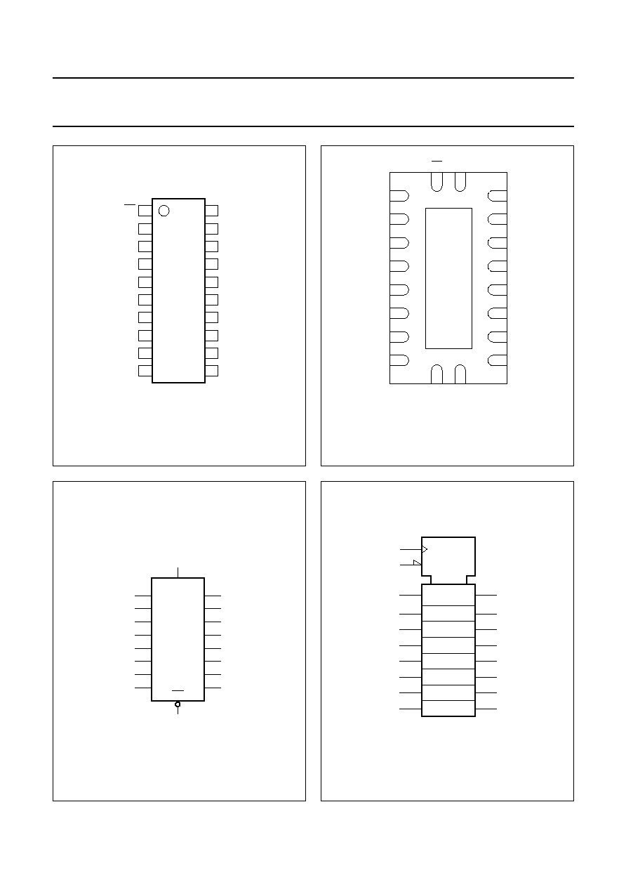
Fig.1 Pin configuration SO20 and TSSOP20.
handbook, halfpage
MR
Q0
D0
D1
Q1
Q2
D2
D3
Q3
GND
VCC
Q7
D7
D6
Q5
D5
Q6
D4
Q4
CP
1
2
3
4
5
6
7
8
9
10
11
12
20
19
18
17
16
15
14
13
273
MNA459
Fig.2 Pin configuration DHVQFN20.
handbook, halfpage
1
2
3
4
5
6
7
8
9
Q0
D0
D1
Q1
Q2
D2
D3
Q3
19
18
17
16
15
14
13
12
Q7
D7
D6
Q6
Q5
D5
D4
Q4
20
MR
VCC
10
11
GND
Top view
CP
GND
(1)
MNB035
(1) The die substrate is attached to this pad using conductive die
attach material. It can not be used as a supply pin or input.
Fig.3 Logic symbol.
handbook, halfpage
MNA460
D0
D1
D2
D3
D4
D5
D6
D7
MR
CP
Q0
Q1
Q2
Q3
Q4
Q5
Q6
Q7
11
1
19
16
15
12
9
6
5
2
18
17
14
13
8
7
4
3
Fig.4 IEC logic symbol.
handbook, halfpage
MNA461
19
16
15
12
9
6
5
11
C1
1
R
1D
2
18
17
14
13
8
7
4
3

