 | –≠–ª–µ–∫—Ç—Ä–æ–Ω–Ω—ã–π –∫–æ–º–ø–æ–Ω–µ–Ω—Ç: 74AHC595D | –°–∫–∞—á–∞—Ç—å:  PDF PDF  ZIP ZIP |

DATA SHEET
Product specification
File under Integrated Circuits, IC06
2000 Mar 15
INTEGRATED CIRCUITS
74AHC595; 74AHCT595
8-bit serial-in/serial or parallel-out
shift register with output latches;
3-state
2000 Mar 15
2
Philips Semiconductors
Product specification
8-bit serial-in/serial or parallel-out shift
register with output latches; 3-state
74AHC595; 74AHCT595
FEATURES
∑
ESD protection:
HBM EIA/JESD22-A114-A exceeds 2000 V
MM EIA/JESD22-A115-A exceeds 200 V
CDM EIA/JESD22-C101 exceeds 1000 V
∑
Balanced propagation delays
∑
All inputs have Schmitt-trigger actions
∑
Inputs accept voltages higher than V
CC
∑
For AHC only: operates with CMOS input levels
∑
For AHCT only: operates with TTL input levels
∑
Specified from
-
40 to +85
∞
C and from
-
40 to +125
∞
C.
APPLICATIONS
∑
Serial-to-parallel data conversion
∑
Remote control holding register.
DESCRIPTION
The 74AHC/AHCT595 are high-speed Si-gate CMOS
devices and are pin compatible with Low power Schottky
TTL (LSTTL). They are specified in compliance with
JEDEC standard No. 7A.
The 74AHC/AHCT595 is an 8-stage serial shift register
with a storage register and 3-state outputs. The shift
register has separate clocks.
Data is shifted on the positive-going transitions of the
SH
CP
input. The data in each register is transferred to the
storage register on a positive-going transition of the ST
CP
input. If both clocks are connected together, the shift
register will always be one clock pulse ahead of the
storage register.
The shift register has a serial input (D
S
) and a serial
standard output (Q
7
') for cascading. It is also provided with
asynchronous reset (active LOW) for all 8 shift register
stages. The storage register has 8 parallel 3-state bus
driver outputs. Data in the storage register appears at the
output whenever the output enable input (OE) is LOW.
QUICK REFERENCE DATA
GND = 0 V; T
amb
= 25
∞
C; t
r
= t
f
3.0 ns.
Notes
1. C
PD
is used to determine the dynamic power dissipation (P
D
in
µ
W).
P
D
= C
PD
◊
V
CC
2
◊
f
i
+
(C
L
◊
V
CC
2
◊
f
o
) where:
f
i
= input frequency in MHz;
f
o
= output frequency in MHz;
(C
L
◊
V
CC
2
◊
f
o
) = sum of outputs;
C
L
= output load capacitance in pF;
V
CC
= supply voltage in Volts.
2. The condition is V
I
= GND to V
CC
.
3. All 9 outputs switching.
SYMBOL
PARAMETER
CONDITIONS
TYPICAL
UNIT
AHC
AHCT
t
PHL
/t
PLH
propagation delay
C
L
= 15 pF; V
CC
= 5 V
SH
CP
to Q
7
'
4.0
3.8
ns
ST
CP
to Q
n
4.2
4.0
ns
MR to Q
7
'
4.4
4.6
ns
C
I
input capacitance
3.0
3.0
pF
f
max
maximum clock frequency
170
170
MHz
C
PD
power dissipation capacitance
C
L
= 50 pF; f = 1 MHz; notes 1, 2 and 3 180
190
pF
2000 Mar 15
3
Philips Semiconductors
Product specification
8-bit serial-in/serial or parallel-out shift
register with output latches; 3-state
74AHC595; 74AHCT595
FUNCTION TABLE
See note 1.
Note
1. H = HIGH voltage level;
L = LOW voltage level;
= LOW-to-HIGH transition;
= HIGH-to-LOW transition;
X = don't care;
NC = no change;
Z = high impedance OFF-state.
ORDERING INFORMATION
INPUT
OUTPUT
FUNCTION
SH
CP
ST
CP
OE
MR
D
S
Q
7
'
Q
n
X
X
L
L
X
L
NC
a LOW level on MR only affects the shift registers
X
L
L
X
L
L
empty shift register loaded into storage register
X
X
H
L
X
L
Z
shift register clear. Parallel outputs in high impedance
OFF-state.
X
L
H
H
Q
6
'
NC
logic HIGH level shifted into shift register stage 0.
Contents of all shift register stages shifted through, e.g.
previous state of stage 6 (internal Q
6
') appears on the
serial output (Q
7
').
X
L
H
X
NC
Q
n
'
contents of shift register stages (internal Q
n
') are
transferred to the storage register and parallel output
stages
L
H
X
Q
6
'
Q
n
'
contents of shift register shifted through. Previous
contents of the shift register is transferred to the storage
register and the parallel output stages.
TYPE NUMBER
PACKAGES
TEMPERATURE
RANGE
PINS
PACKAGE
MATERIAL
CODE
74AHC595D
-
40 to +125
∞
C
16
SO
plastic
SOT109-1
74AHC595PW
16
TSSOP
plastic
SOT403-1
74AHCT595D
16
SO
plastic
SOT109-1
74AHCT595PW
16
TSSOP
plastic
SOT403-1
2000 Mar 15
4
Philips Semiconductors
Product specification
8-bit serial-in/serial or parallel-out shift
register with output latches; 3-state
74AHC595; 74AHCT595
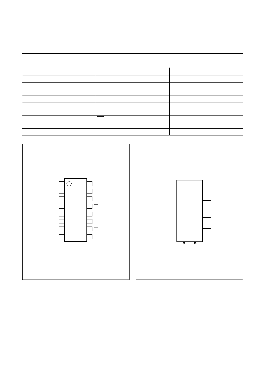
PINNING
PIN
SYMBOL
DESCRIPTION
1, 2, 3, 4, 5, 6, 7 and 15
Q
1
, Q
2
, Q
3
, Q
4
, Q
5
, Q
6
, Q
7
and Q
0
parallel data output
8
GND
ground (0 V)
9
Q
7
'
serial data output
10
MR
master reset (active LOW)
11
SH
CP
shift register clock input
12
ST
CP
storage register clock input
13
OE
output enable input (active LOW)
14
D
S
serial data input
16
V
CC
DC supply voltage
handbook, halfpage
Q1
Q2
Q3
Q4
Q5
Q6
Q7
GND
VCC
Q0
DS
OE
SHCP
STCP
Q7'
1
2
3
4
5
6
7
8
16
15
14
13
12
11
10
9
595
MNA551
MR
Fig.1 Pin configuration.
handbook, halfpage
OE
MR
9
15
1
2
3
4
5
6
7
13
10
14
11
12
MNA552
Q1
Q0
Q2
Q3
Q4
Q5
Q6
Q7
Q7'
DS
STCP
SHCP
Fig.2 Logic symbol.
2000 Mar 15
5
Philips Semiconductors
Product specification
8-bit serial-in/serial or parallel-out shift
register with output latches; 3-state
74AHC595; 74AHCT595
handbook, halfpage
MNA553
15
9
1
2
3
4
5
6
7
1D
2D
C1/
10
11
14
C2
12
13
EN3
SRG8
R
3
Fig.3 IEC logic symbol.
handbook, halfpage
MNA554
3-STATE OUTPUTS
8-BIT STORAGE REGISTER
8-STAGE SHIFT REGISTER
Q0 Q1 Q2 Q3 Q4 Q5 Q6 Q7
Q7'
14
15
1
2
3
4
5
6
7
9
DS
SHCP
STCP
OE
11
10
12
13
MR
Fig.4 Functional diagram.
handbook, full pagewidth
STAGE 0
STAGES 1 TO 6
STAGE 7
FF0
D
CP
Q
R
LATCH
D
CP
Q
FF7
D
CP
Q
R
LATCH
D
CP
Q
MNA555
D
Q
Q1 Q2 Q3 Q4 Q5 Q6
Q7
Q7'
Q0
DS
STCP
SHCP
OE
MR
Fig.5 Logic diagram.
2000 Mar 15
6
Philips Semiconductors
Product specification
8-bit serial-in/serial or parallel-out shift
register with output latches; 3-state
74AHC595; 74AHCT595
handbook, full pagewidth
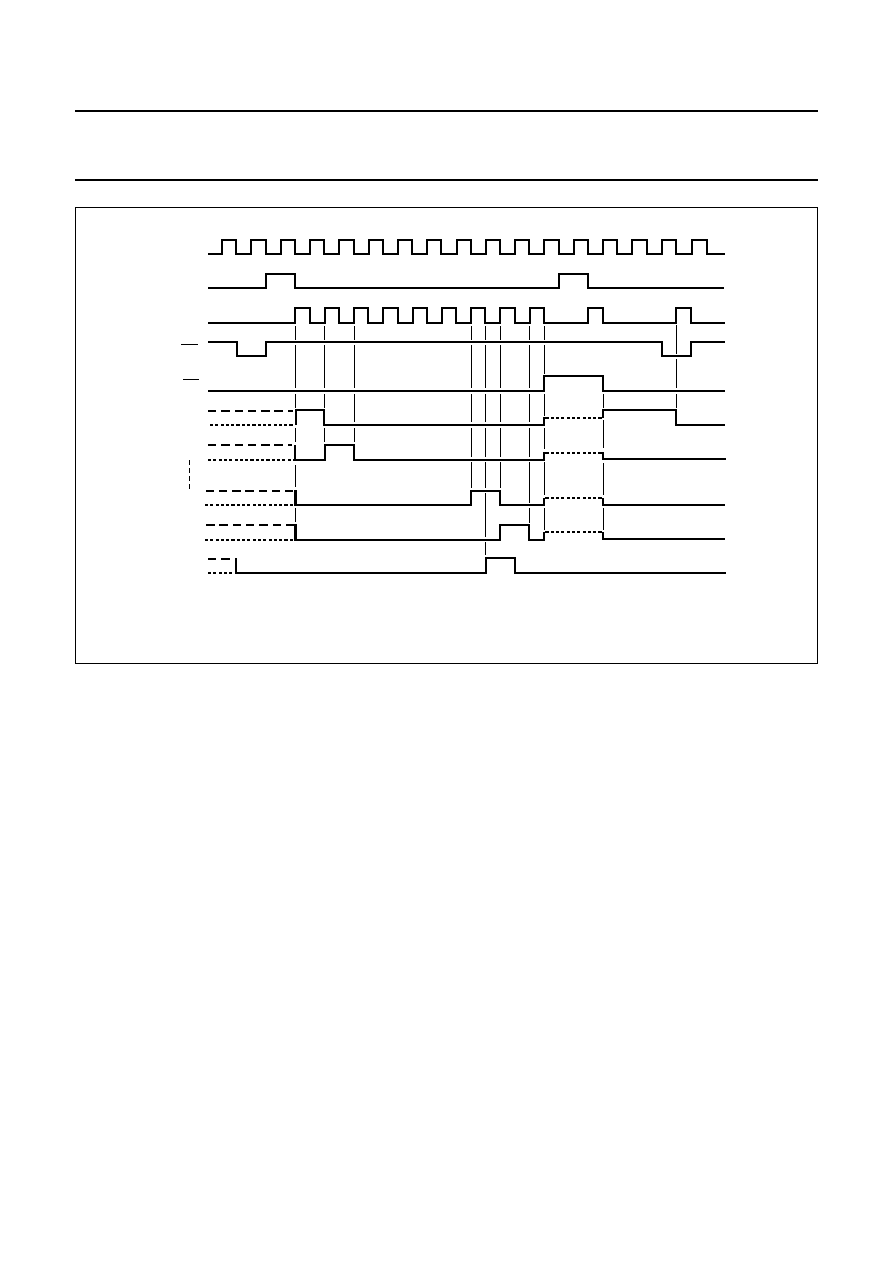
SHCP
DS
STCP
MR
OE
Q0
Q1
Q6
Q7
Q7'
Z-state
Z-state
Z-state
Z-state
MNA556
Fig.6 Timing diagram.
2000 Mar 15
7
Philips Semiconductors
Product specification
8-bit serial-in/serial or parallel-out shift
register with output latches; 3-state
74AHC595; 74AHCT595
RECOMMENDED OPERATING CONDITIONS
LIMITING VALUES
In accordance with the Absolute Maximum Rating System (IEC 60134); voltages are referenced to GND (ground = 0 V).
Notes
1. The input and output voltage ratings may be exceeded if the input and output current ratings are observed.
2. For SO packages: above 70
∞
C the value of P
D
derates linearly with 8 mW/K.
For TSSOP packages: above 60
∞
C the value of P
D
derates linearly with 5.5 mW/K.
SYMBOL
PARAMETER
CONDITIONS
74AHC
74AHCT
UNIT
MIN.
TYP.
MAX.
MIN.
TYP.
MAX.
V
CC
DC supply voltage
2.0
5.0
5.5
4.5
5.0
5.5
V
V
I
input voltage
0
-
5.5
0
-
5.5
V
V
O
output voltage
0
-
V
CC
0
-
V
CC
V
T
amb
operating ambient temperature
see DC and AC
characteristics per
device
-
40
+25
+85
-
40
+25
+85
∞
C
-
40
+25
+125
-
40
+25
+125
∞
C
t
r
, t
f
input rise and fall ratios (
t/
V)
V
CC
= 3.3
±
0.3 V
-
-
100
-
-
-
ns/V
V
CC
= 5
±
0.5 V
-
-
20
-
-
20
ns/V
SYMBOL
PARAMETER
CONDITIONS
MIN.
MAX. UNIT
V
CC
DC supply voltage
-
0.5
+7.0
V
V
I
input voltage
-
0.5
+7.0
V
I
IK
DC input diode current
V
I
<
-
0.5 V; note 1
-
-
20
mA
I
OK
DC output clamping diode
current
-
0.5 > V
O
> V
CC
+ 0.5 V; note 1
-
±
20
mA
I
O
DC output sink current
-
0.5 < V
O
< V
CC
+ 0.5 V
-
±
25
mA
I
CC
DC V
CC
or GND current
-
±
75
mA
T
stg
storage temperature
-
65
+150
∞
C
P
D
power dissipation per package
for temperature range:
-
40 to +125
∞
C; note 2
-
500
mW
2000 Mar 15
8
Philips Semiconductors
Product specification
8-bit serial-in/serial or parallel-out shift
register with output latches; 3-state
74AHC595; 74AHCT595
DC CHARACTERISTICS
74AHC family
Over recommended operating conditions; voltages are referenced to GND (ground = 0 V).
SYMBOL
PARAMETER
TEST CONDITIONS
T
amb
(
∞
C)
UNIT
OTHER
V
CC
(V)
25
-
40 to +85
-
40 to +125
MIN.
TYP.
MAX. MIN. MAX. MIN. MAX.
V
IH
HIGH-level input
voltage
2.0
1.5
-
-
1.5
-
1.5
-
V
3.0
2.1
-
-
2.1
-
2.1
-
V
5.5
3.85
-
-
3.85
-
3.85
-
V
V
IL
LOW-level input
voltage
2.0
-
-
0.5
-
0.5
-
0.5
V
3.0
-
-
0.9
-
0.9
-
0.9
V
5.5
-
-
1.65
-
1.65
-
1.65
V
V
OH
HIGH-level output
voltage
V
I
= V
IH
or V
IL
;
I
O
=
-
50
µ
A
2.0
1.9
2.0
-
1.9
-
1.9
-
V
3.0
2.9
3.0
-
2.9
-
2.9
-
V
4.5
4.4
4.5
-
4.4
-
4.4
-
V
V
I
= V
IH
or V
IL
;
I
O
=
-
4.0 mA
3.0
2.58
-
-
2.48
-
2.40
-
V
V
I
= V
IH
or V
IL
;
I
O
=
-
8.0 mA
4.5
3.94
-
-
3.8
-
3.70
-
V
V
OL
LOW-level output
voltage
V
I
= V
IH
or V
IL
;
I
O
= 50
µ
A
2.0
-
0
0.1
-
0.1
-
0.1
V
3.0
-
0
0.1
-
0.1
-
0.1
V
4.5
-
0
0.1
-
0.1
-
0.1
V
V
I
= V
IH
or V
IL
;
I
O
= 4.0 mA
3.0
-
-
0.36
-
0.44
-
0.55
V
V
I
= V
IH
or V
IL
;
I
O
= 8.0 mA
4.5
-
-
0.36
-
0.44
-
0.55
V
I
I
input leakage
current
V
I
= V
CC
or GND
5.5
-
-
0.1
-
1.0
-
2.0
µ
A
I
OZ
3-state output
OFF-state current
V
I
= V
IH
or V
IL
;
V
O
= V
CC
or GND
5.5
-
-
±
0.25
-
±
2.5
-
±
10.0
µ
A
I
CC
quiescent supply
current
V
I
= V
CC
or GND;
I
O
= 0
5.5
-
-
4.0
-
40
-
80
µ
A
C
I
input capacitance
-
-
3
10
-
10
-
10
pF

2000 Mar 15
9
Philips Semiconductors
Product specification
8-bit serial-in/serial or parallel-out shift
register with output latches; 3-state
74AHC595; 74AHCT595
74AHCT family
Over recommended operating conditions; voltages are referenced to GND (ground = 0 V).
SYMBOL
PARAMETER
TEST CONDITIONS
T
amb
(
∞
C)
UNIT
OTHER
V
CC
(V)
25
-
40 to +85
-
40 to +125
MIN.
TYP. MAX. MIN. MAX. MIN. MAX.
V
IH
HIGH-level input
voltage
4.5 to 5.5 2.0
-
-
2.0
-
2.0
-
V
V
IL
LOW-level input
voltage
4.5 to 5.5
-
-
0.8
-
0.8
-
0.8
V
V
OH
HIGH-level output
voltage
V
I
= V
IH
or V
IL
;
I
O
=
-
50
µ
A
4.5
4.4
4.5
-
4.4
-
4.4
-
V
V
I
= V
IH
or V
IL
;
I
O
=
-
8.0 mA
4.5
3.94
-
-
3.8
-
3.70
-
V
V
OL
LOW-level output
voltage
V
I
= V
IH
or V
IL
;
I
O
= 50
µ
A
4.5
-
0
0.1
-
0.1
-
0.1
V
V
I
= V
IH
or V
IL
;
I
O
= 8.0 mA
4.5
-
-
0.36
-
0.44
-
0.55
V
I
I
input leakage
current
V
I
= V
IH
or V
IL
5.5
-
-
0.1
-
1.0
-
2.0
µ
A
I
OZ
3-state output
OFF-state current
V
I
= V
IH
or V
IL
;
V
O
= V
CC
or GND
per input pin;
other inputs at
V
CC
or GND;
I
O
= 0
5.5
-
-
±
0.25
-
±
2.5
-
±
10.0
µ
A
I
CC
quiescent supply
current
V
I
= V
CC
or GND;
I
O
= 0
5.5
-
-
4.0
-
40
-
80
µ
A
I
CC
additional
quiescent supply
current per input
pin
V
I
= V
CC
-
2.1 V
other inputs at
V
CC
or GND;
I
O
= 0
4.5 to 5.5
-
-
1.35
-
1.5
-
1.5
mA
C
I
input capacitance
-
-
3
10
-
10
-
10
pF

2000 Mar 15
10
Philips Semiconductors
Product specification
8-bit serial-in/serial or parallel-out shift
register with output latches; 3-state
74AHC595; 74AHCT595
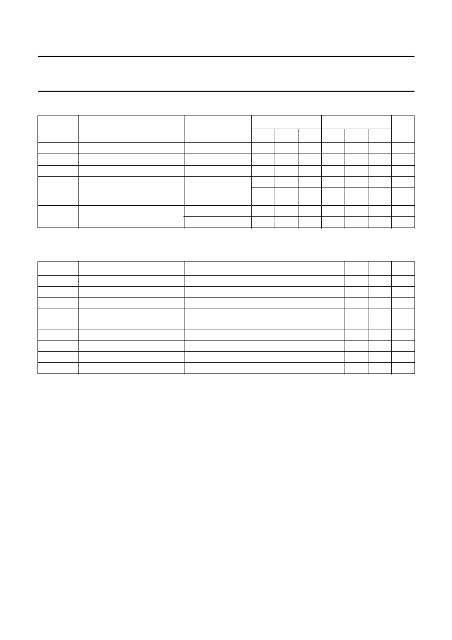
AC CHARACTERISTICS
Type 74AHC595
GND = 0 V; t
r
= t
f
3.0 ns.
SYMBOL
PARAMETER
TEST CONDITIONS
T
amb
(
∞
C)
UNIT
WAVEFORMS
C
L
25
-
40 to +85
-
40 to +125
MIN.
TYP.
MAX.
MIN.
MAX.
MIN.
MAX.
V
CC
= 3.0 to 3.6 V; note 1
t
PHL
/t
PLH
propagation delay
SH
CP
to Q
7
'
see Figs 7
and 12
15 pF
-
5.7
13.0
1.0
15.0
1.0
16.5
ns
propagation delay
ST
CP
to Q
n
see Figs 8
and 12
-
5.9
11.9
1.0
13.5
1.0
15.0
ns
t
PHL
propagation delay
MR to Q
7
'
see Figs 10
and 12
-
5.9
12.8
1.0
13.7
1.0
15.0
ns
t
PZH
/t
PZL
3-state output enable
time OE to Q
n
see Figs 11
and 12
-
5.6
11.5
1.0
13.5
1.0
15.0
ns
t
PHZ
/t
PLZ
3-state output disable
time OE to Q
n
-
5.4
11.0
1.0
13.0
1.0
14.5
ns
t
PHL
/t
PLH
propagation delay
SH
CP
to Q
7
'
see Figs 7
and 12
50 pF
-
7.7
16.5
1.0
18.5
1.0
20.1
ns
propagation delay
ST
CP
to Q
n
see Figs 8
and 12
-
7.7
15.4
1.0
17.0
1.0
18.5
ns
t
PHL
propagation delay
MR to Q
7
'
see Figs 10
and 12
-
7.4
16.3
1.0
17.2
1.0
18.7
ns
t
PZH
/t
PZL
3-state output enable
time OE to Q
n
see Figs 11
and 12
-
7.4
15.0
1.0
17.0
1.0
18.5
ns
t
PHZ
/t
PLZ
3-state output disable
time OE to Q
n
-
8.7
15.7
1.0
16.2
1.0
17.5
ns
t
W
shift clock pulse width
HIGH or LOW
see Figs 7
and 12
5.0
-
-
5.0
-
5.0
-
ns
storage clock pulse
width HIGH or LOW
see Figs 8
and 12
5.0
-
-
5.0
-
5.0
-
ns
master reset pulse
width LOW
see Figs 10
and 12
5.0
-
-
5.0
-
5.0
-
ns
t
su
set-up time
D
S
to SH
CP
see Figs 8
and 12
3.5
-
-
3.5
-
3.5
-
ns
set-up time
SH
CP
to ST
CP
see Figs 9
and 12
8.5
-
-
8.5
-
8.5
-
ns
t
h
hold time
D
S
to SH
CP
1.5
-
-
1.5
-
1.5
-
ns
t
rem
removal time
MR to SH
CP
see Figs 10
and 12
3.0
-
-
3.0
-
3.0
-
ns
f
max
maximum clock pulse
frequency
SH
CP
or ST
CP
see Figs 7, 8
and 12
80
125
-
60
-
40
-
MHz
2000 Mar 15
11
Philips Semiconductors
Product specification
8-bit serial-in/serial or parallel-out shift
register with output latches; 3-state
74AHC595; 74AHCT595
Notes
1. Typical values at V
CC
= 3.3 V.
2. Typical values at V
CC
= 5.0 V.
V
CC
= 4.5 to 5.5 V; note 2
t
PHL
/t
PLH
propagation delay
SH
CP
to Q
7
'
see Figs 7
and 12
15 pF
-
4.0
8.2
1.0
9.4
1.0
10.5
ns
propagation delay
ST
CP
to Q
n
see Figs 8
and 12
-
4.2
7.4
1.0
8.5
1.0
9.5
ns
t
PHL
propagation delay
MR to Q
7
'
see Figs 10
and 12
-
4.4
8.0
1.0
9.1
1.0
10.0
ns
t
PZH
/t
PZL
3-state output enable
time OE to Q
n
see Figs 11
and 12
-
4.0
8.6
1.0
10.0
1.0
11.0
ns
t
PHZ
/t
PLZ
3-state output disable
time OE to Q
n
-
3.8
8.0
1.0
9.5
1.0
10.5
ns
t
PHL
/t
PLH
propagation delay
SH
CP
to Q
7
'
see Figs 7
and 12
50 pF
-
5.4
10.0
1.0
11.4
1.0
12.5
ns
propagation delay
ST
CP
to Q
n
see Figs 8
and 12
-
5.5
9.0
1.0
10.5
1.0
11.5
ns
t
PHL
propagation delay
MR to Q
7
'
see Figs 10
and 12
-
5.6
10.0
1.0
11.1
1.0
12.0
ns
t
PZH
/t
PZL
3-state output enable
time OE to Q
n
see Figs 11
and 12
-
5.3
10.6
1.0
12.0
1.0
13.0
ns
t
PHZ
/t
PLZ
3-state output disable
time OE to Q
n
-
5.8
10.3
1.0
11.0
1.0
12.0
ns
t
W
shift clock pulse width
HIGH or LOW
see Figs 7
and 12
5.0
-
-
5.0
-
5.0
-
ns
storage clock pulse
width HIGH or LOW
see Figs 8
and 12
5.0
-
-
5.0
-
5.0
-
ns
master reset pulse
width LOW
see Figs 10
and 12
5.0
-
-
5.0
-
5.0
-
ns
t
su
set-up time
D
S
to SH
CP
see Figs 8
and 12
3.0
-
-
3.0
-
3.0
-
ns
set-up time
SH
CP
to ST
CP
see Figs 9
and 12
5.0
-
-
5.0
-
5.0
-
ns
t
h
hold time
D
S
to SH
CP
2.0
-
-
2.0
-
2.0
-
ns
t
rem
removal time
MR to SH
CP
see Figs 10
and 12
2.5
-
-
2.5
-
2.5
-
ns
f
max
maximum clock pulse
frequency
SH
CP
or ST
CP
see Figs 7, 8
and 12
130
170
-
110
-
90
-
MHz
SYMBOL
PARAMETER
TEST CONDITIONS
T
amb
(
∞
C)
UNIT
WAVEFORMS
C
L
25
-
40 to +85
-
40 to +125
MIN.
TYP.
MAX.
MIN.
MAX.
MIN.
MAX.
2000 Mar 15
12
Philips Semiconductors
Product specification
8-bit serial-in/serial or parallel-out shift
register with output latches; 3-state
74AHC595; 74AHCT595
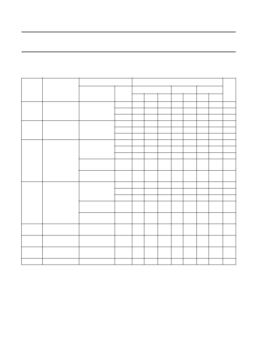
Type 74AHCT595
GND = 0 V; t
r
= t
f
3.0 ns.
Note
1. Typical values at V
CC
= 5.0 V.
SYMBOL
PARAMETER
TEST CONDITIONS
T
amb
(
∞
C)
UNIT
WAVEFORMS
C
L
25
-
40 to +85
-
40 to +125
MIN.
TYP.
MAX.
MIN.
MAX.
MIN.
MAX.
V
CC
= 4.5 to 5.5 V; note 1
t
PHL
/t
PLH
propagation delay
SH
CP
to Q
7
'
see Figs 7
and 12
15 pF
-
3.8
8.2
1.0
9.0
1.0
10.0
ns
propagation delay
ST
CP
to Q
n
see Figs 8
and 12
-
4.0
7.4
1.0
8.5
1.0
9.5
ns
t
PHL
propagation delay
MR to Q
7
'
see Figs 10
and 12
-
4.6
8.2
1.0
9.5
1.0
10.5
ns
t
PZH
/t
PZL
3-state output enable
time OE to Q
n
see Figs 11
and 12
-
4.8
9.0
1.0
11.0
1.0
12.0
ns
t
PHZ
/t
PLZ
3-state output disable
time OE to Q
n
-
3.6
6.9
1.0
8.0
1.0
9.0
ns
t
PHL
/t
PLH
propagation delay
SH
CP
to Q
7
'
see Figs 7
and 12
50 pF
-
5.2
10.0
1.0
11.0
1.0
12.0
ns
propagation delay
ST
CP
to Q
n
see Figs 8
and 12
-
5.3
9.0
1.0
10.5
1.0
11.5
ns
t
PHL
propagation delay
MR to Q
7
'
see Figs 10
and 12
-
5.8
10.5
1.0
11.5
1.0
12.5
ns
t
PZH
/t
PZL
3-state output enable
time OE to Q
n
see Figs 11
and 12
-
6.2
11.6
1.0
13.0
1.0
14.5
ns
t
PHZ
/t
PLZ
3-state output disable
time OE to Q
n
-
5.8
10.3
1.0
11.0
1.0
12.0
ns
t
W
shift clock pulse width
HIGH or LOW
see Figs 7
and 12
5.0
-
-
5.0
-
5.0
-
ns
storage clock pulse
width HIGH or LOW
see Figs 8
and 12
5.0
-
-
5.0
-
5.0
-
ns
master reset pulse
width LOW
see Figs 10
and 12
5.0
-
-
5.0
-
5.0
-
ns
t
su
set-up time
SH
CP
to ST
CP
see Figs 8
and 12
5.0
-
-
5.0
-
5.0
-
ns
set-up time
D
S
to SH
CP
see Figs 9
and 12
3.0
-
-
3.0
-
3.0
-
ns
t
h
hold time
D
S
to SH
CP
2.0
-
-
2.0
-
2.0
-
ns
t
rem
removal time
MR to SH
CP
see Figs 10
and 12
3.0
-
-
3.0
-
3.0
-
ns
f
max
maximum clock pulse
frequency
SH
CP
or ST
CP
see Figs 7, 8
and 12
130
170
-
110
-
90
-
MHz
2000 Mar 15
13
Philips Semiconductors
Product specification
8-bit serial-in/serial or parallel-out shift
register with output latches; 3-state
74AHC595; 74AHCT595
AC WAVEFORMS
handbook, full pagewidth
MNA557
SHCP input
Q7' output
tPLH
tPHL
tW
1/fmax
VM
(2)
VOH
VI
GND
VOL
VM
(1)
FAMILY
V
I
INPUT
REQUIREMENTS
V
M
(1)
INPUT
V
M
(2)
OUTPUT
AHC
GND to V
CC
50% V
CC
50% V
CC
AHCT
GND to 3.0 V
1.5 V
50% V
CC
Fig.7
The clock (SH
CP
) to output (Q
7'
) propagation delays, the shift clock pulse width (t
W
) and maximum shift
clock frequency (f
max
).
handbook, full pagewidth
MNA558
STCP input
Qn output
tPLH
tPHL
tW
tsu
1/fmax
VM
(2)
VOH
VI
GND
VOL
VM
(1)
SHCP input
VI
GND
VM
(1)
Fig.8
The storage clock (ST
CP
) to output (Q
n
) propagation delays, the storage clock pulse width (t
W
) and the
shift clock to storage clock set-up time (t
su
).
FAMILY
V
I
INPUT
REQUIREMENTS
V
M
(1)
INPUT
V
M
(2)
OUTPUT
AHC
GND to V
CC
50% V
CC
50% V
CC
AHCT
GND to 3.0 V
1.5 V
50% V
CC
2000 Mar 15
14
Philips Semiconductors
Product specification
8-bit serial-in/serial or parallel-out shift
register with output latches; 3-state
74AHC595; 74AHCT595
handbook, full pagewidth
MNA560
GND
GND
th
tsu
th
tsu
VM
(1)
VM
(1)
VM
(2)
VI
VOH
VOL
VI
Q7' output
SHCP input
DS input
Fig.9 The data set-up (t
su
) and hold (t
h
) times for the D
S
input.
FAMILY
V
I
INPUT
REQUIREMENTS
V
M
(1)
INPUT
V
M
(2)
OUTPUT
AHC
GND to V
CC
50% V
CC
50% V
CC
AHCT
GND to 3.0 V
1.5 V
50% V
CC
The shaded areas indicate when the input is permitted to change for
predictable output performance.
handbook, full pagewidth
MNA561
MR input
SHCP input
Q7' output
tPHL
tW
trem
VM
(2)
VOH
VOL
VI
GND
VI
GND
VM
(1)
VM
(1)
FAMILY
V
I
INPUT
REQUIREMENTS
V
M
(1)
INPUT
V
M
(2)
OUTPUT
AHC
GND to V
CC
50% V
CC
50% V
CC
AHCT
GND to 3.0 V
1.5 V
50% V
CC
Fig.10 The master reset (MR) pulse width, the master reset to output (Q
7'
) propagation delays and the master
reset to shift clock (SH
CP
) removal time (t
rem
).
2000 Mar 15
15
Philips Semiconductors
Product specification
8-bit serial-in/serial or parallel-out shift
register with output latches; 3-state
74AHC595; 74AHCT595
Fig.11 3-state enable and disable times.
FAMILY
V
I
INPUT
REQUIREMENTS
V
M
(1)
INPUT
V
M
(2)
OUTPUT
AHC
GND to V
CC
50% V
CC
50% V
CC
AHCT
GND to 3.0 V
1.5 V
50% V
CC
handbook, full pagewidth
MNA450
tPLZ
tPHZ
outputs
disabled
outputs
enabled
VOH
-
0.3 V
VOL
+
0.3 V
outputs
enabled
output
LOW-to-OFF
OFF-to-LOW
output
HIGH-to-OFF
OFF-to-HIGH
OE input
VI
VCC
VM
(1)
VOL
VOH
GND
GND
tPZL
tPZH
VM
(2)
VM
(2)
handbook, full pagewidth
open
GND
VCC
VCC
VI
VO
MNA219
D.U.T.
CL
RT
1000
PULSE
GENERATOR
S1
Fig.12 Load circuitry for switching times.
TEST
S1
t
PLH
/t
PHL
open
t
PLZ
/t
PZL
V
CC
t
PHZ
/t
PZH
GND
Definitions for test circuit.
C
L
= load capacitance including jig and probe capacitance (See Chapter "AC characteristics").
R
T
= termination resistance should be equal to the output impedance Z
o
of the pulse generator.
2000 Mar 15
16
Philips Semiconductors
Product specification
8-bit serial-in/serial or parallel-out shift
register with output latches; 3-state
74AHC595; 74AHCT595
PACKAGE OUTLINES
X
w
M
A
A
1
A
2
b
p
D
H
E
L
p
Q
detail X
E
Z
e
c
L
v
M
A
(A )
3
A
8
9
1
16
y
pin 1 index
UNIT
A
max.
A
1
A
2
A
3
b
p
c
D
(1)
E
(1)
(1)
e
H
E
L
L
p
Q
Z
y
w
v
REFERENCES
OUTLINE
VERSION
EUROPEAN
PROJECTION
ISSUE DATE
IEC
JEDEC
EIAJ
mm
inches
1.75
0.25
0.10
1.45
1.25
0.25
0.49
0.36
0.25
0.19
10.0
9.8
4.0
3.8
1.27
6.2
5.8
0.7
0.6
0.7
0.3
8
0
o
o
0.25
0.1
DIMENSIONS (inch dimensions are derived from the original mm dimensions)
Note
1. Plastic or metal protrusions of 0.15 mm maximum per side are not included.
1.0
0.4
SOT109-1
97-05-22
99-12-27
076E07
MS-012
0.069
0.010
0.004
0.057
0.049
0.01
0.019
0.014
0.0100
0.0075
0.39
0.38
0.16
0.15
0.050
1.05
0.041
0.244
0.228
0.028
0.020
0.028
0.012
0.01
0.25
0.01
0.004
0.039
0.016
0
2.5
5 mm
scale
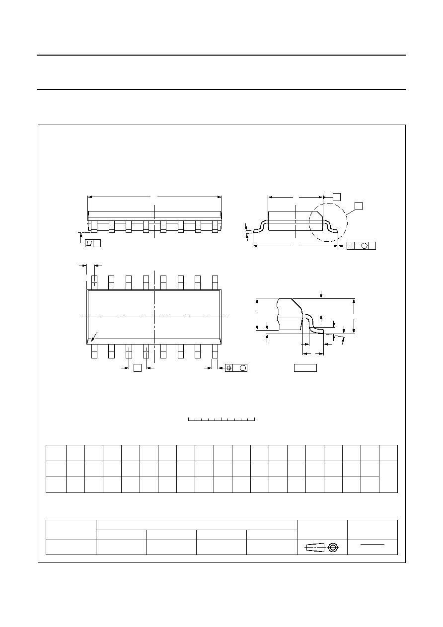
SO16: plastic small outline package; 16 leads; body width 3.9 mm
SOT109-1
2000 Mar 15
17
Philips Semiconductors
Product specification
8-bit serial-in/serial or parallel-out shift
register with output latches; 3-state
74AHC595; 74AHCT595
UNIT
A
1
A
2
A
3
b
p
c
D
(1)
E
(2)
(1)
e
H
E
L
L
p
Q
Z
y
w
v
REFERENCES
OUTLINE
VERSION
EUROPEAN
PROJECTION
ISSUE DATE
IEC
JEDEC
EIAJ
mm
0.15
0.05
0.95
0.80
0.30
0.19
0.2
0.1
5.1
4.9
4.5
4.3
0.65
6.6
6.2
0.4
0.3
0.40
0.06
8
0
o
o
0.13
0.1
0.2
1.0
DIMENSIONS (mm are the original dimensions)
Notes
1. Plastic or metal protrusions of 0.15 mm maximum per side are not included.
2. Plastic interlead protrusions of 0.25 mm maximum per side are not included.
0.75
0.50
SOT403-1
MO-153
95-04-04
99-12-27
w
M
b
p
D
Z
e
0.25
1
8
16
9
A
A
1
A
2
L
p
Q
detail X
L
(A )
3
H
E
E
c
v
M
A
X
A
y
0
2.5
5 mm
scale
TSSOP16: plastic thin shrink small outline package; 16 leads; body width 4.4 mm
SOT403-1
A
max.
1.10
pin 1 index

2000 Mar 15
18
Philips Semiconductors
Product specification
8-bit serial-in/serial or parallel-out shift
register with output latches; 3-state
74AHC595; 74AHCT595
SOLDERING
Introduction to soldering surface mount packages
This text gives a very brief insight to a complex technology.
A more in-depth account of soldering ICs can be found in
our
"Data Handbook IC26; Integrated Circuit Packages"
(document order number 9398 652 90011).
There is no soldering method that is ideal for all surface
mount IC packages. Wave soldering is not always suitable
for surface mount ICs, or for printed-circuit boards with
high population densities. In these situations reflow
soldering is often used.
Reflow soldering
Reflow soldering requires solder paste (a suspension of
fine solder particles, flux and binding agent) to be applied
to the printed-circuit board by screen printing, stencilling or
pressure-syringe dispensing before package placement.
Several methods exist for reflowing; for example,
infrared/convection heating in a conveyor type oven.
Throughput times (preheating, soldering and cooling) vary
between 100 and 200 seconds depending on heating
method.
Typical reflow peak temperatures range from
215 to 250
∞
C. The top-surface temperature of the
packages should preferable be kept below 230
∞
C.
Wave soldering
Conventional single wave soldering is not recommended
for surface mount devices (SMDs) or printed-circuit boards
with a high component density, as solder bridging and
non-wetting can present major problems.
To overcome these problems the double-wave soldering
method was specifically developed.
If wave soldering is used the following conditions must be
observed for optimal results:
∑
Use a double-wave soldering method comprising a
turbulent wave with high upward pressure followed by a
smooth laminar wave.
∑
For packages with leads on two sides and a pitch (e):
≠ larger than or equal to 1.27 mm, the footprint
longitudinal axis is preferred to be parallel to the
transport direction of the printed-circuit board;
≠ smaller than 1.27 mm, the footprint longitudinal axis
must be parallel to the transport direction of the
printed-circuit board.
The footprint must incorporate solder thieves at the
downstream end.
∑
For packages with leads on four sides, the footprint must
be placed at a 45
∞
angle to the transport direction of the
printed-circuit board. The footprint must incorporate
solder thieves downstream and at the side corners.
During placement and before soldering, the package must
be fixed with a droplet of adhesive. The adhesive can be
applied by screen printing, pin transfer or syringe
dispensing. The package can be soldered after the
adhesive is cured.
Typical dwell time is 4 seconds at 250
∞
C.
A mildly-activated flux will eliminate the need for removal
of corrosive residues in most applications.
Manual soldering
Fix the component by first soldering two
diagonally-opposite end leads. Use a low voltage (24 V or
less) soldering iron applied to the flat part of the lead.
Contact time must be limited to 10 seconds at up to
300
∞
C.
When using a dedicated tool, all other leads can be
soldered in one operation within 2 to 5 seconds between
270 and 320
∞
C.
2000 Mar 15
19
Philips Semiconductors
Product specification
8-bit serial-in/serial or parallel-out shift
register with output latches; 3-state
74AHC595; 74AHCT595
Suitability of surface mount IC packages for wave and reflow soldering methods
Notes
1. All surface mount (SMD) packages are moisture sensitive. Depending upon the moisture content, the maximum
temperature (with respect to time) and body size of the package, there is a risk that internal or external package
cracks may occur due to vaporization of the moisture in them (the so called popcorn effect). For details, refer to the
Drypack information in the
"Data Handbook IC26; Integrated Circuit Packages; Section: Packing Methods".
2. These packages are not suitable for wave soldering as a solder joint between the printed-circuit board and heatsink
(at bottom version) can not be achieved, and as solder may stick to the heatsink (on top version).
3. If wave soldering is considered, then the package must be placed at a 45
∞
angle to the solder wave direction.
The package footprint must incorporate solder thieves downstream and at the side corners.
4. Wave soldering is only suitable for LQFP, TQFP and QFP packages with a pitch (e) equal to or larger than 0.8 mm;
it is definitely not suitable for packages with a pitch (e) equal to or smaller than 0.65 mm.
5. Wave soldering is only suitable for SSOP and TSSOP packages with a pitch (e) equal to or larger than 0.65 mm; it is
definitely not suitable for packages with a pitch (e) equal to or smaller than 0.5 mm.
DEFINITIONS
LIFE SUPPORT APPLICATIONS
These products are not designed for use in life support appliances, devices, or systems where malfunction of these
products can reasonably be expected to result in personal injury. Philips customers using or selling these products for
use in such applications do so at their own risk and agree to fully indemnify Philips for any damages resulting from such
improper use or sale.
PACKAGE
SOLDERING METHOD
WAVE
REFLOW
(1)
BGA, LFBGA, SQFP, TFBGA
not suitable
suitable
HLQFP, HSQFP, HSOP, HTQFP, HTSSOP, SMS
not suitable
(2)
suitable
PLCC
(3)
, SO, SOJ
suitable
suitable
LQFP, QFP, TQFP
not recommended
(3)(4)
suitable
SSOP, TSSOP, VSO
not recommended
(5)
suitable
Data sheet status
Objective specification
This data sheet contains target or goal specifications for product development.
Preliminary specification
This data sheet contains preliminary data; supplementary data may be published later.
Product specification
This data sheet contains final product specifications.
Limiting values
Limiting values given are in accordance with the Absolute Maximum Rating System (IEC 60134). Stress above one or
more of the limiting values may cause permanent damage to the device. These are stress ratings only and operation
of the device at these or at any other conditions above those given in the Characteristics sections of the specification
is not implied. Exposure to limiting values for extended periods may affect device reliability.
Application information
Where application information is given, it is advisory and does not form part of the specification.

© Philips Electronics N.V.
SCA
All rights are reserved. Reproduction in whole or in part is prohibited without the prior written consent of the copyright owner.
The information presented in this document does not form part of any quotation or contract, is believed to be accurate and reliable and may be changed
without notice. No liability will be accepted by the publisher for any consequence of its use. Publication thereof does not convey nor imply any license
under patent- or other industrial or intellectual property rights.
Internet: http://www.semiconductors.philips.com
2000
69
Philips Semiconductors ≠ a worldwide company
For all other countries apply to: Philips Semiconductors,
International Marketing & Sales Communications, Building BE-p, P.O. Box 218,
5600 MD EINDHOVEN, The Netherlands, Fax. +31 40 27 24825
Argentina: see South America
Australia: 3 Figtree Drive, HOMEBUSH, NSW 2140,
Tel. +61 2 9704 8141, Fax. +61 2 9704 8139
Austria: Computerstr. 6, A-1101 WIEN, P.O. Box 213,
Tel. +43 1 60 101 1248, Fax. +43 1 60 101 1210
Belarus: Hotel Minsk Business Center, Bld. 3, r. 1211, Volodarski Str. 6,
220050 MINSK, Tel. +375 172 20 0733, Fax. +375 172 20 0773
Belgium: see The Netherlands
Brazil: see South America
Bulgaria: Philips Bulgaria Ltd., Energoproject, 15th floor,
51 James Bourchier Blvd., 1407 SOFIA,
Tel. +359 2 68 9211, Fax. +359 2 68 9102
Canada: PHILIPS SEMICONDUCTORS/COMPONENTS,
Tel. +1 800 234 7381, Fax. +1 800 943 0087
China/Hong Kong: 501 Hong Kong Industrial Technology Centre,
72 Tat Chee Avenue, Kowloon Tong, HONG KONG,
Tel. +852 2319 7888, Fax. +852 2319 7700
Colombia: see South America
Czech Republic: see Austria
Denmark: Sydhavnsgade 23, 1780 COPENHAGEN V,
Tel. +45 33 29 3333, Fax. +45 33 29 3905
Finland: Sinikalliontie 3, FIN-02630 ESPOO,
Tel. +358 9 615 800, Fax. +358 9 6158 0920
France: 51 Rue Carnot, BP317, 92156 SURESNES Cedex,
Tel. +33 1 4099 6161, Fax. +33 1 4099 6427
Germany: Hammerbrookstraþe 69, D-20097 HAMBURG,
Tel. +49 40 2353 60, Fax. +49 40 2353 6300
Hungary: see Austria
India: Philips INDIA Ltd, Band Box Building, 2nd floor,
254-D, Dr. Annie Besant Road, Worli, MUMBAI 400 025,
Tel. +91 22 493 8541, Fax. +91 22 493 0966
Indonesia: PT Philips Development Corporation, Semiconductors Division,
Gedung Philips, Jl. Buncit Raya Kav.99-100, JAKARTA 12510,
Tel. +62 21 794 0040 ext. 2501, Fax. +62 21 794 0080
Ireland: Newstead, Clonskeagh, DUBLIN 14,
Tel. +353 1 7640 000, Fax. +353 1 7640 200
Israel: RAPAC Electronics, 7 Kehilat Saloniki St, PO Box 18053,
TEL AVIV 61180, Tel. +972 3 645 0444, Fax. +972 3 649 1007
Italy: PHILIPS SEMICONDUCTORS, Via Casati, 23 - 20052 MONZA (MI),
Tel. +39 039 203 6838, Fax +39 039 203 6800
Japan: Philips Bldg 13-37, Kohnan 2-chome, Minato-ku,
TOKYO 108-8507, Tel. +81 3 3740 5130, Fax. +81 3 3740 5057
Korea: Philips House, 260-199 Itaewon-dong, Yongsan-ku, SEOUL,
Tel. +82 2 709 1412, Fax. +82 2 709 1415
Malaysia: No. 76 Jalan Universiti, 46200 PETALING JAYA, SELANGOR,
Tel. +60 3 750 5214, Fax. +60 3 757 4880
Mexico: 5900 Gateway East, Suite 200, EL PASO, TEXAS 79905,
Tel. +9-5 800 234 7381, Fax +9-5 800 943 0087
Middle East: see Italy
Netherlands: Postbus 90050, 5600 PB EINDHOVEN, Bldg. VB,
Tel. +31 40 27 82785, Fax. +31 40 27 88399
New Zealand: 2 Wagener Place, C.P.O. Box 1041, AUCKLAND,
Tel. +64 9 849 4160, Fax. +64 9 849 7811
Norway: Box 1, Manglerud 0612, OSLO,
Tel. +47 22 74 8000, Fax. +47 22 74 8341
Pakistan: see Singapore
Philippines: Philips Semiconductors Philippines Inc.,
106 Valero St. Salcedo Village, P.O. Box 2108 MCC, MAKATI,
Metro MANILA, Tel. +63 2 816 6380, Fax. +63 2 817 3474
Poland: Al.Jerozolimskie 195 B, 02-222 WARSAW,
Tel. +48 22 5710 000, Fax. +48 22 5710 001
Portugal: see Spain
Romania: see Italy
Russia: Philips Russia, Ul. Usatcheva 35A, 119048 MOSCOW,
Tel. +7 095 755 6918, Fax. +7 095 755 6919
Singapore: Lorong 1, Toa Payoh, SINGAPORE 319762,
Tel. +65 350 2538, Fax. +65 251 6500
Slovakia: see Austria
Slovenia: see Italy
South Africa: S.A. PHILIPS Pty Ltd., 195-215 Main Road Martindale,
2092 JOHANNESBURG, P.O. Box 58088 Newville 2114,
Tel. +27 11 471 5401, Fax. +27 11 471 5398
South America: Al. Vicente Pinzon, 173, 6th floor,
04547-130 S√O PAULO, SP, Brazil,
Tel. +55 11 821 2333, Fax. +55 11 821 2382
Spain: Balmes 22, 08007 BARCELONA,
Tel. +34 93 301 6312, Fax. +34 93 301 4107
Sweden: Kottbygatan 7, Akalla, S-16485 STOCKHOLM,
Tel. +46 8 5985 2000, Fax. +46 8 5985 2745
Switzerland: Allmendstrasse 140, CH-8027 ZÐRICH,
Tel. +41 1 488 2741 Fax. +41 1 488 3263
Taiwan: Philips Semiconductors, 6F, No. 96, Chien Kuo N. Rd., Sec. 1,
TAIPEI, Taiwan Tel. +886 2 2134 2886, Fax. +886 2 2134 2874
Thailand: PHILIPS ELECTRONICS (THAILAND) Ltd.,
209/2 Sanpavuth-Bangna Road Prakanong, BANGKOK 10260,
Tel. +66 2 745 4090, Fax. +66 2 398 0793
Turkey: Yukari Dudullu, Org. San. Blg., 2.Cad. Nr. 28 81260 Umraniye,
ISTANBUL, Tel. +90 216 522 1500, Fax. +90 216 522 1813
Ukraine: PHILIPS UKRAINE, 4 Patrice Lumumba str., Building B, Floor 7,
252042 KIEV, Tel. +380 44 264 2776, Fax. +380 44 268 0461
United Kingdom: Philips Semiconductors Ltd., 276 Bath Road, Hayes,
MIDDLESEX UB3 5BX, Tel. +44 208 730 5000, Fax. +44 208 754 8421
United States: 811 East Arques Avenue, SUNNYVALE, CA 94088-3409,
Tel. +1 800 234 7381, Fax. +1 800 943 0087
Uruguay: see South America
Vietnam: see Singapore
Yugoslavia: PHILIPS, Trg N. Pasica 5/v, 11000 BEOGRAD,
Tel. +381 11 3341 299, Fax.+381 11 3342 553
Printed in The Netherlands
613507/01/pp
20
Date of release:
2000 Mar 15
Document order number:
9397 750 06822