74AHC14; 74AHCT14 Hex inverting Schmitt trigger
DATA SHEET
Product specification
Supersedes data of 1999 Sep 27
2003 May 26
INTEGRATED CIRCUITS
74AHC14; 74AHCT14
Hex inverting Schmitt trigger
2003 May 26
2
Philips Semiconductors
Product specification
Hex inverting Schmitt trigger
74AHC14; 74AHCT14
FEATURES
·
Balanced propagation delays
·
Inputs accepts voltages higher than V
CC
·
For 74AHC only: operates with CMOS input levels
·
For 74AHCT only: operates with TTL input levels
·
ESD protection:
HBM EIA/JESD22-A114-A exceeds 2000 V
MM EIA/JESD22-A115-A exceeds 200 V.
·
Specified from
-
40 to +85
°
C and
-
40 to +125
°
C.
DESCRIPTION
The 74AHC14 and 74AHCT14 are high-speed Si-gate
CMOS devices and are pin compatible with low power
Schottky TTL (LSTTL). They are specified in compliance
with JEDEC standard No. 7A.
The 74AHC14 and 74AHCT14 provide six inverting buffers
with Schmitt-trigger action. They are capable of
transforming slowly changing input signals into sharply
defined, jitter-free output signals.
QUICK REFERENCE DATA
GND = 0 V; T
amb
= 25
°
C; t
r
= t
f
3.0 ns.
Notes
1. C
PD
is used to determine the dynamic power dissipation (P
D
in
µ
W).
P
D
= C
PD
×
V
CC
2
×
f
i
×
N +
(C
L
×
V
CC
2
×
f
o
) where:
f
i
= input frequency in MHz;
f
o
= output frequency in MHz;
C
L
= output load capacitance in pF;
V
CC
= supply voltage in Volts;
N = total load switching outputs;
(C
L
×
V
CC
2
×
f
o
) = sum of the outputs.
2. The condition is V
I
= GND to V
CC
.
FUNCTION TABLE
See note 1.
Note
1. H = HIGH voltage level;
L = LOW voltage level.
SYMBOL
PARAMETER
CONDITIONS
TYPICAL
UNIT
AHC
AHCT
t
PHL
/t
PLH
propagation delay nA to nY
C
L
= 15 pF; V
CC
= 5 V
3.2
4.0
ns
C
I
input capacitance
V
I
= V
CC
or GND
3.0
3.0
pF
C
O
output capacitance
4.0
4.0
pF
C
PD
power dissipation capacitance per
buffer
C
L
= 50 pF; f = 1 MHz;
notes 1 and 2
10
12
pF
INPUT
OUTPUT
nA
nY
L
H
H
L
2003 May 26
3
Philips Semiconductors
Product specification
Hex inverting Schmitt trigger
74AHC14; 74AHCT14
ORDERING INFORMATION
TYPE NUMBER
PACKAGE
TEMPERATURE
RANGE
PINS
PACKAGE
MATERIAL
CODE
74AHC14D
-
40 to +125
°
C
14
SO14
plastic
SOT108-1
74AHCT14D
-
40 to +125
°
C
14
SO14
plastic
SOT108-1
74AHC14PW
-
40 to +125
°
C
14
TSSOP14
plastic
SOT402-1
74AHCT14PW
-
40 to +125
°
C
14
TSSOP14
plastic
SOT402-1
74AHC14BQ
-
40 to +125
°
C
14
DHVQFN14
plastic
SOT762-1
74AHCT14BQ
-
40 to +125
°
C
14
DHVQFN14
plastic
SOT762-1
PINNING
PIN
SYMBOL
DESCRIPTION
1
1A
data input
2
1Y
data output
3
2A
data input
4
2Y
data output
5
3A
data input
6
3Y
data output
7
GND
ground (0 V)
8
4Y
data output
9
4A
data input
10
5Y
data output
11
5A
data input
12
6Y
data output
13
6A
data input
14
V
CC
supply voltage
PIN
SYMBOL
DESCRIPTION
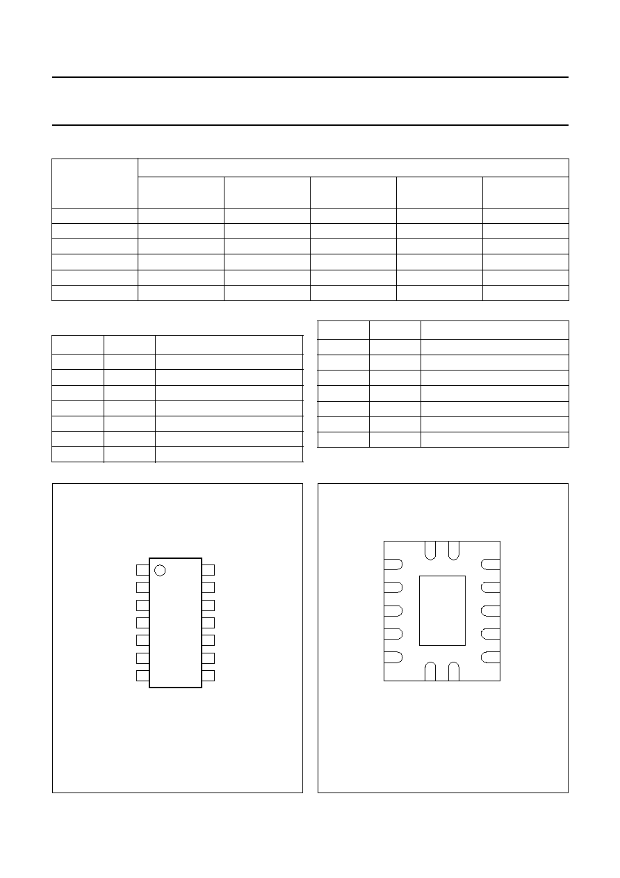
Fig.1 Pin configuration SO14 and TSSOP14.
handbook, halfpage
MNA203
14
1
2
3
4
5
6
7
8
14
13
12
11
10
9
1A
1Y
2A
2Y
3A
3Y
GND
4Y
4A
5Y
5A
6Y
6A
VCC
Fig.2 Pin configuration DHVQFN14.
handbook, halfpage
1
14
GND
(1)
1A
VCC
7
2
3
4
5
6
1Y
2A
2Y
3A
3Y
13
12
11
10
9
6A
6Y
5A
5Y
4A
8
GND
Top view
4Y
MCE196
(1) The die substrate is attached to this pad using conductive die
attach material. It can not be used as a supply pin or input.
2003 May 26
4
Philips Semiconductors
Product specification
Hex inverting Schmitt trigger
74AHC14; 74AHCT14
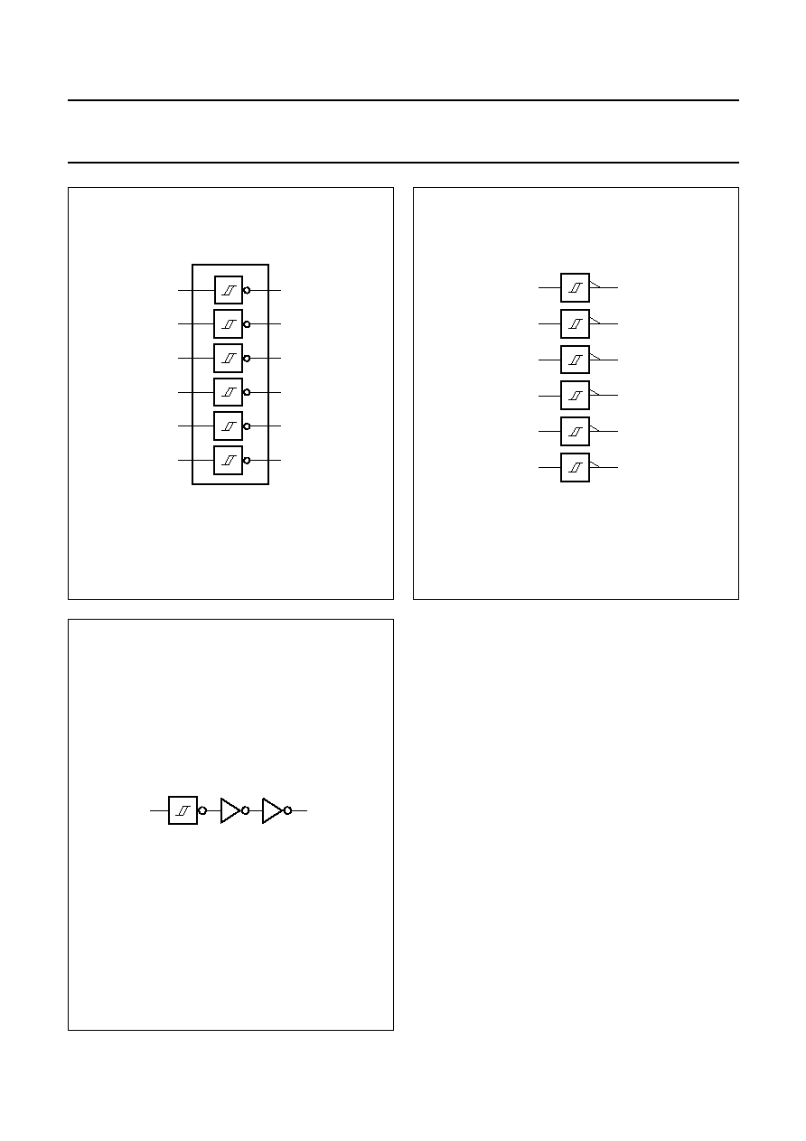
Fig.3 Logic symbol.
handbook, halfpage
MNA204
1A
1Y
1
2
2A
2Y
3
4
3A
3Y
5
6
4A
4Y
9
8
5A
5Y
11
10
6A
6Y
13
12
Fig.4 IEC logic symbol.
handbook, halfpage
2
1
MNB034
4
3
6
5
8
9
10
11
12
13
Fig.5 Logic diagram (one Schmitt trigger).
handbook, halfpage
MNA205
A
Y
2003 May 26
5
Philips Semiconductors
Product specification
Hex inverting Schmitt trigger
74AHC14; 74AHCT14
RECOMMENDED OPERATING CONDITIONS
LIMITING VALUES
In accordance with the Absolute Maximum Rating System (IEC 60134); voltages are referenced to GND (ground = 0 V).
Notes
1. The input and output voltage ratings may be exceeded if the input and output current ratings are observed.
2. For SO14 packages: above 70
°
C the value of P
D
derates linearly with 8 mW/K.
For TSSOP14 packages: above 60
°
C the value of P
D
derates linearly with 5.5 mW/K.
For DHVQFN14 packages: above 60
°
C the value of P
D
derates linearly with 4.5 mW/K.
SYMBOL
PARAMETER
CONDITIONS
74AHC
74AHCT
UNIT
MIN.
TYP.
MAX.
MIN.
TYP.
MAX.
V
CC
supply voltage
2.0
5.0
5.5
4.5
5.0
5.5
V
V
I
input voltage
0
-
5.5
0
-
5.5
V
V
O
output voltage
0
-
V
CC
0
-
V
CC
V
T
amb
operating ambient temperature
see DC and AC
characteristics per
device
-
+25
-
-
+25
-
°
C
-
40
-
+125
-
40
-
+125
°
C
-
40
-
+125
-
40
-
+125
°
C
SYMBOL
PARAMETER
CONDITIONS
MIN.
MAX. UNIT
V
CC
supply voltage
-
0.5
+7.0
V
V
I
input voltage
-
0.5
+7.0
V
I
IK
input diode current
V
I
<
-
0.5 V; note 1
-
-
20
mA
I
OK
output diode current
V
O
<
-
0.5 V or V
O
> V
CC
+ 0.5 V; note 1
-
±
20
mA
I
O
output source or sink current
-
0.5 V < V
O
< V
CC
+ 0.5 V
-
±
25
mA
I
CC
, I
GND
V
CC
or GND current
-
±
75
mA
T
stg
storage temperature
-
65
+150
°
C
P
D
power dissipation
T
amb
=
-
40 to +125
°
C; note 2
-
500
mW
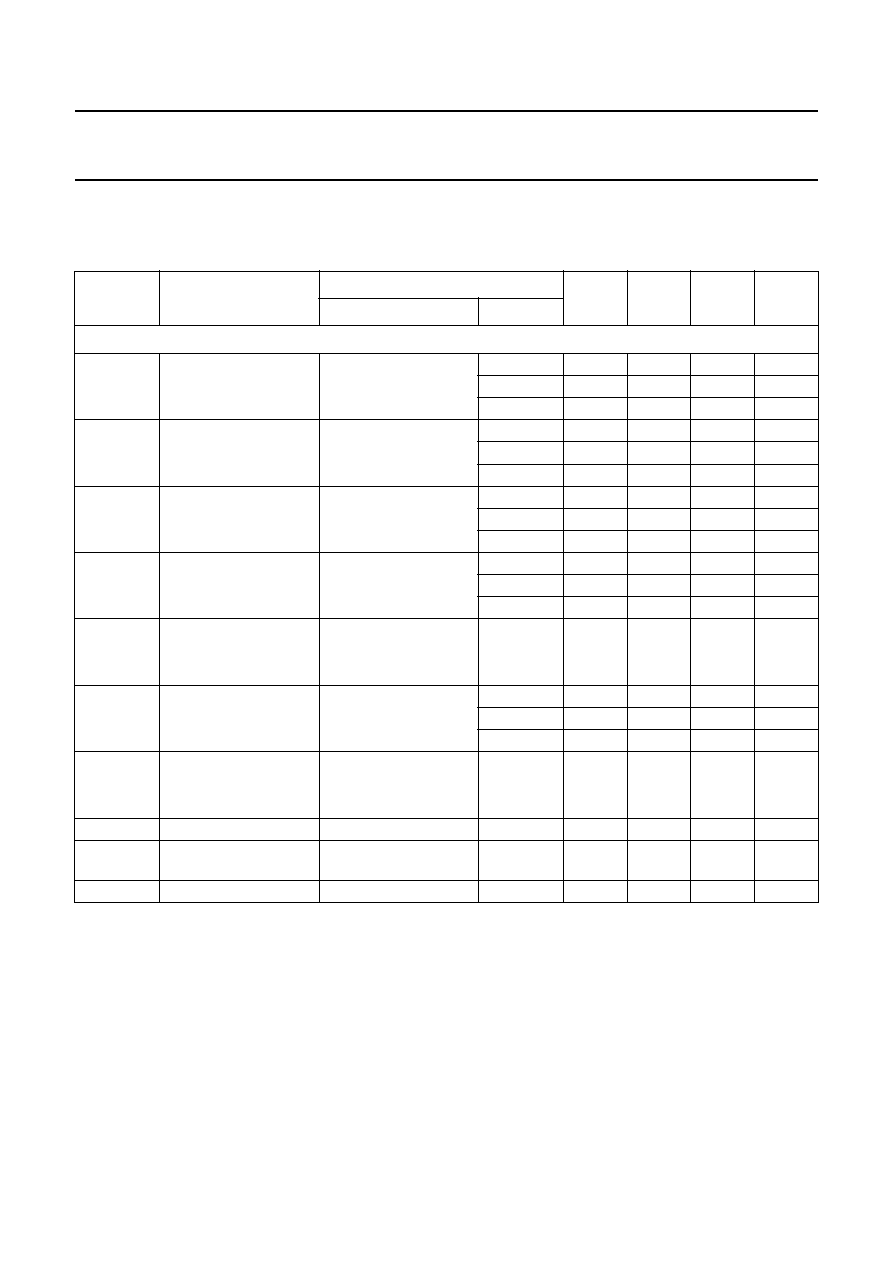
2003 May 26
6
Philips Semiconductors
Product specification
Hex inverting Schmitt trigger
74AHC14; 74AHCT14
DC CHARACTERISTICS
Type 74AHC14
At recommended operating conditions; voltage are referenced to GND (ground = 0 V).
SYMBOL
PARAMETER
TEST CONDITIONS
MIN.
TYP.
MAX.
UNIT
OTHER
V
CC
(V)
T
amb
= 25
°
C
V
T+
positive going threshold
3.0
-
-
2.2
V
4.5
-
-
3.15
V
5.5
-
-
3.85
V
V
T
-
negative going
threshold
3.0
0.9
-
-
V
4.5
1.35
-
-
V
5.5
1.65
-
-
V
V
H
hysteresis (V
T+
-
V
T
-
)
3.0
0.3
-
1.2
V
4.5
0.4
-
1.4
V
5.5
0.5
-
1.6
V
V
OH
HIGH-level output
voltage; all outputs
V
I
= V
IH
or V
IL
;
I
O
=
-
50
µ
A
2.0
1.9
2.0
-
V
3.0
2.9
3.0
-
V
4.5
4.4
4.5
-
V
V
OH
HIGH-level output
voltage
V
I
= V
IH
or V
IL
I
O
=
-
4.0 mA
3.0
2.58
-
-
V
I
O
=
-
8.0 mA
4.5
3.94
-
-
V
V
OL
LOW-level output
voltage; all outputs
V
I
= V
IH
or V
IL
;
I
O
= 50
µ
A
2.0
-
0
0.1
V
3.0
-
0
0.1
V
4.5
-
0
0.1
V
V
OL
LOW-level output
voltage
V
I
= V
IH
or V
IL
I
O
= 4.0 mA
3.0
-
-
0.36
V
I
O
= 8.0 mA
4.5
-
-
0.36
V
I
LI
input leakage current
V
I
= V
CC
or GND
5.5
-
-
0.1
µ
A
I
CC
quiescent supply
current
V
I
= V
CC
or GND;
I
O
= 0
5.5
-
-
2.0
µ
A
C
I
input capacitance
-
3
10
pF
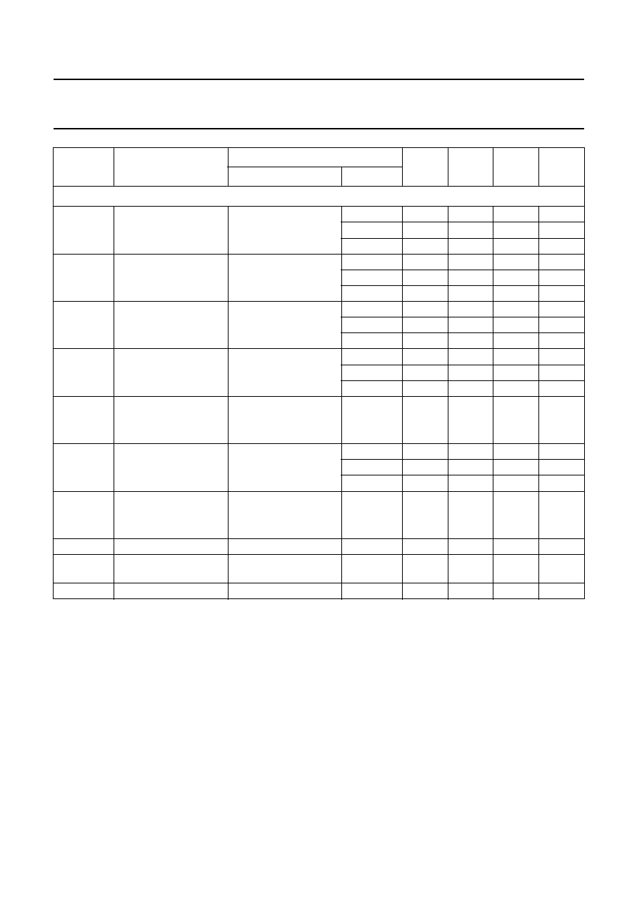
2003 May 26
7
Philips Semiconductors
Product specification
Hex inverting Schmitt trigger
74AHC14; 74AHCT14
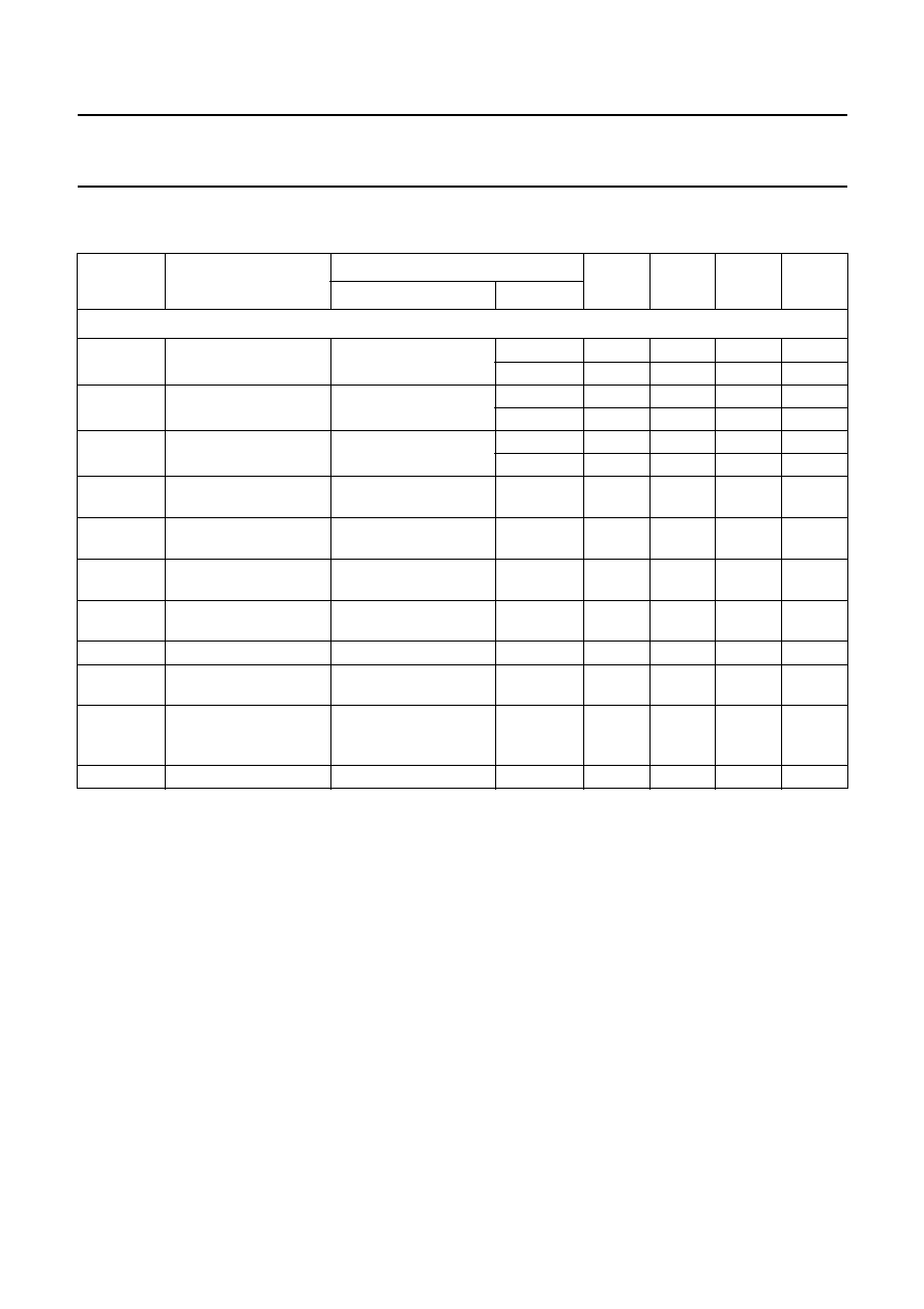
T
amb
=
-
40 to +85
°
C
V
T+
positive going threshold
3.0
-
-
2.2
V
4.5
-
-
3.15
V
5.5
-
-
3.85
V
V
T
-
negative going
threshold
3.0
0.9
-
-
V
4.5
1.35
-
-
V
5.5
1.65
-
-
V
V
H
hysteresis (V
T+
-
V
T
-
)
3.0
0.3
-
1.2
V
4.5
0.4
-
1.4
V
5.5
0.5
-
1.6
V
V
OH
HIGH-level output
voltage; all outputs
V
I
= V
IH
or V
IL
;
I
O
=
-
50
µ
A
2.0
1.9
-
-
V
3.0
2.9
-
-
V
4.5
4.4
-
-
V
V
OH
HIGH-level output
voltage
V
I
= V
IH
or V
IL
I
O
=
-
4.0 mA
3.0
2.48
-
-
V
I
O
=
-
8.0 mA
4.5
3.8
-
-
V
V
OL
LOW-level output
voltage; all outputs
V
I
= V
IH
or V
IL
;
I
O
= 50
µ
A
2.0
-
-
0.1
V
3.0
-
-
0.1
V
4.5
-
-
0.1
V
V
OL
LOW-level output
voltage
V
I
= V
IH
or V
IL
I
O
= 4.0 mA
3.0
-
-
0.44
V
I
O
= 8.0 mA
4.5
-
-
0.44
V
I
LI
input leakage current
V
I
= V
CC
or GND
5.5
-
-
1.0
µ
A
I
CC
quiescent supply
current
V
I
= V
CC
or GND;
I
O
= 0
5.5
-
-
20
µ
A
C
I
input capacitance
-
-
10
pF
SYMBOL
PARAMETER
TEST CONDITIONS
MIN.
TYP.
MAX.
UNIT
OTHER
V
CC
(V)

2003 May 26
8
Philips Semiconductors
Product specification
Hex inverting Schmitt trigger
74AHC14; 74AHCT14
T
amb
=
-
40 to +125
°
C
V
T+
positive going threshold
3.0
-
-
2.2
V
4.5
-
-
3.15
V
5.5
-
-
3.85
V
V
T
-
negative going
threshold
3.0
0.9
-
-
V
4.5
1.35
-
-
V
5.5
1.65
-
-
V
V
H
hysteresis (V
T+
-
V
T
-
)
3.0
0.25
-
1.2
V
4.5
0.35
-
1.4
V
5.5
0.45
-
1.6
V
V
OH
HIGH-level output
voltage; all outputs
V
I
= V
IH
or V
IL
;
I
O
=
-
50
µ
A
2.0
1.9
-
-
V
3.0
2.9
-
-
V
4.5
4.4
-
-
V
V
OH
HIGH-level output
voltage
V
I
= V
IH
or V
IL
I
O
=
-
4.0 mA
3.0
2.40
-
-
V
I
O
=
-
8.0 mA
4.5
3.70
-
-
V
V
OL
LOW-level output
voltage; all outputs
V
I
= V
IH
or V
IL
;
I
O
= 50
µ
A
2.0
-
-
0.1
V
3.0
-
-
0.1
V
4.5
-
-
0.1
V
V
OL
LOW-level output
voltage
V
I
= V
IH
or V
IL
I
O
= 4.0 mA
3.0
-
-
0.55
V
I
O
= 8.0 mA
4.5
-
-
0.55
V
I
LI
input leakage current
V
I
= V
CC
or GND
5.5
-
-
2.0
µ
A
I
CC
quiescent supply
current
V
I
= V
CC
or GND;
I
O
= 0
5.5
-
-
40
µ
A
C
I
input capacitance
-
-
10
pF
SYMBOL
PARAMETER
TEST CONDITIONS
MIN.
TYP.
MAX.
UNIT
OTHER
V
CC
(V)
2003 May 26
9
Philips Semiconductors
Product specification
Hex inverting Schmitt trigger
74AHC14; 74AHCT14
Type 74AHCT14
At recommended operating conditions; voltage are referenced to GND (ground = 0 V).
SYMBOL
PARAMETER
TEST CONDITIONS
MIN.
TYP.
MAX.
UNIT
OTHER
V
CC
(V)
T
amb
= 25
°
C
V
T+
positive going threshold
4.5
-
-
1.9
V
5.5
-
-
2.1
V
V
T
-
negative going
threshold
4.5
0.5
-
-
V
5.5
0.6
-
-
V
V
H
hysteresis (V
T+
-
V
T
-
)
4.5
0.4
-
1.4
V
5.5
0.4
-
1.5
V
V
OH
HIGH-level output
voltage; all outputs
V
I
= V
IH
or V
IL
;
I
O
=
-
50
µ
A
4.5
4.4
4.5
-
V
V
OH
HIGH-level output
voltage
V
I
= V
IH
or V
IL
;
I
O
=
-
8.0 mA
4.5
3.94
-
-
V
V
OL
LOW-level output
voltage; all outputs
V
I
= V
IH
or V
IL
;
I
O
= 50
µ
A
4.5
-
0
0.1
V
V
OL
LOW-level output
voltage
V
I
= V
IH
or V
IL
;
I
O
= 8 mA
4.5
-
-
0.36
V
I
LI
input leakage current
V
I
= V
CC
or GND
5.5
-
-
0.1
µ
A
I
CC
quiescent supply
current
V
I
= V
CC
or GND;
I
O
= 0
5.5
-
-
2.0
µ
A
I
CC
additional quiescent
supply current per input
pin
V
I
= V
CC
-
2.1 V other
inputs at V
CC
or GND;
I
O
= 0
4.5 to 5.5
-
-
1.35
mA
C
I
input capacitance
-
3
10
pF

2003 May 26
10
Philips Semiconductors
Product specification
Hex inverting Schmitt trigger
74AHC14; 74AHCT14
T
amb
=
-
40 to +85
°
C
V
T+
positive going threshold
4.5
-
-
1.9
V
5.5
-
-
2.1
V
V
T
-
negative going
threshold
4.5
0.5
-
-
V
5.5
0.6
-
-
V
V
H
hysteresis (V
T+
-
V
T
-
)
4.5
0.4
-
1.4
V
5.5
0.4
-
1.5
V
V
OH
HIGH-level output
voltage; all outputs
V
I
= V
IH
or V
IL
;
I
O
=
-
50
µ
A
4.5
4.4
-
-
V
V
OH
HIGH-level output
voltage
V
I
= V
IH
or V
IL
;
I
O
=
-
8.0 mA
4.5
3.8
-
-
V
V
OL
LOW-level output
voltage; all outputs
V
I
= V
IH
or V
IL
;
I
O
= 50
µ
A
4.5
-
-
0.1
V
V
OL
LOW-level output
voltage
V
I
= V
IH
or V
IL
;
I
O
= 8 mA
4.5
-
-
0.44
V
I
LI
input leakage current
V
I
= V
CC
or GND
5.5
-
-
1.0
µ
A
I
CC
quiescent supply
current
V
I
= V
CC
or GND;
I
O
= 0
5.5
-
-
20
µ
A
I
CC
additional quiescent
supply current per input
pin
V
I
= V
CC
-
2.1 V other
inputs at V
CC
or GND;
I
O
= 0
4.5 to 5.5
-
-
1.5
mA
C
I
input capacitance
-
-
10
pF
SYMBOL
PARAMETER
TEST CONDITIONS
MIN.
TYP.
MAX.
UNIT
OTHER
V
CC
(V)
2003 May 26
11
Philips Semiconductors
Product specification
Hex inverting Schmitt trigger
74AHC14; 74AHCT14
T
amb
=
-
40 to +125
°
C
V
T+
positive going threshold
4.5
-
-
1.9
V
5.5
-
-
2.1
V
V
T
-
negative going
threshold
4.5
0.5
-
-
V
5.5
0.6
-
-
V
V
H
hysteresis (V
T+
-
V
T
-
)
4.5
0.35
-
1.4
V
5.5
0.35
-
1.5
V
V
OH
HIGH-level output
voltage; all outputs
V
I
= V
IH
or V
IL
;
I
O
=
-
50
µ
A
4.5
4.4
-
-
V
V
OH
HIGH-level output
voltage
V
I
= V
IH
or V
IL
;
I
O
=
-
8.0 mA
4.5
3.7
-
-
V
V
OL
LOW-level output
voltage; all outputs
V
I
= V
IH
or V
IL
;
I
O
= 50
µ
A
4.5
-
-
0.1
V
V
OL
LOW-level output
voltage
V
I
= V
IH
or V
IL
;
I
O
= 8 mA
4.5
-
-
0.55
V
I
LI
input leakage current
V
I
= V
CC
or GND
5.5
-
-
2.0
µ
A
I
CC
quiescent supply
current
V
I
= V
CC
or GND;
I
O
= 0
5.5
-
-
40
µ
A
I
CC
additional quiescent
supply current per input
pin
V
I
= V
CC
-
2.1 V other
inputs at V
CC
or GND;
I
O
= 0
4.5 to 5.5
-
-
1.5
mA
C
I
input capacitance
-
-
10
pF
SYMBOL
PARAMETER
TEST CONDITIONS
MIN.
TYP.
MAX.
UNIT
OTHER
V
CC
(V)
2003 May 26
12
Philips Semiconductors
Product specification
Hex inverting Schmitt trigger
74AHC14; 74AHCT14
AC CHARACTERISTICS
Type 74AHC14
GND = 0 V; t
r
= t
f
3.0 ns.
SYMBOL
PARAMETER
TEST CONDITIONS
MIN.
TYP.
MAX.
UNIT
OTHER
C
L
(pF)
V
CC
(V)
T
amb
= 25
°
C
t
PHL
/t
PLH
propagation delay
nA to nY
see Figs 6 and 7
15
3.3
-
4.3
-
ns
15
3.0 to 3.6
-
-
12.8
ns
50
3.3
-
5.8
-
ns
50
3.0 to 3.6
-
-
16.3
ns
15
5.0
-
3.2
-
ns
15
4.5 to 5.5
-
-
8.6
ns
50
5.0
-
4.2
-
ns
50
4.5 to 5.5
-
-
10.6
ns
T
amb
=
-
40 to +85
°
C
t
PHL
/t
PLH
propagation delay
nA to nY
see Figs 6 and 7
15
3.0 to 3.6
1.0
-
15.0
ns
50
3.0 to 3.6
1.0
-
18.0
ns
15
4.5 to 5.5
1.0
-
10.0
ns
50
4.5 to 5.5
1.0
-
12.0
ns
T
amb
=
-
40 to +125
°
C
t
PHL
/t
PLH
propagation delay
nA to nY
see Figs 6 and 7
15
3.0 to 3.6
1.0
-
16.0
ns
50
3.0 to 3.6
1.0
-
20.5
ns
15
4.5 to 5.5
1.0
-
11.0
ns
50
4.5 to 5.5
1.0
-
13.5
ns
2003 May 26
13
Philips Semiconductors
Product specification
Hex inverting Schmitt trigger
74AHC14; 74AHCT14
Type 74AHCT14
GND = 0 V; t
r
= t
f
3.0 ns.
SYMBOL
PARAMETER
TEST CONDITIONS
MIN.
TYP.
MAX.
UNIT
OTHER
C
L
(pF)
V
CC
(V)
T
amb
= 25
°
C
t
PHL
/t
PLH
propagation delay
nA to nY
see Figs 6 and 7
15
5.0
-
4.0
-
ns
15
4.5 to 5.5
-
-
7.0
ns
50
5.0
-
5.4
-
ns
50
4.5 to 5.5
-
-
8.0
ns
T
amb
=
-
40 to +85
°
C
t
PHL
/t
PLH
propagation delay
nA to nY
see Figs 6 and 7
15
4.5 to 5.5
1.0
-
8.0
ns
50
4.5 to 5.5
1.0
-
9.0
ns
T
amb
=
-
40 to +125
°
C
t
PHL
/t
PLH
propagation delay
nA to nY
see Figs 6 and 7
15
4.5 to 5.5
1.0
-
9.0
ns
50
4.5 to 5.5
1.0
-
10.0
ns
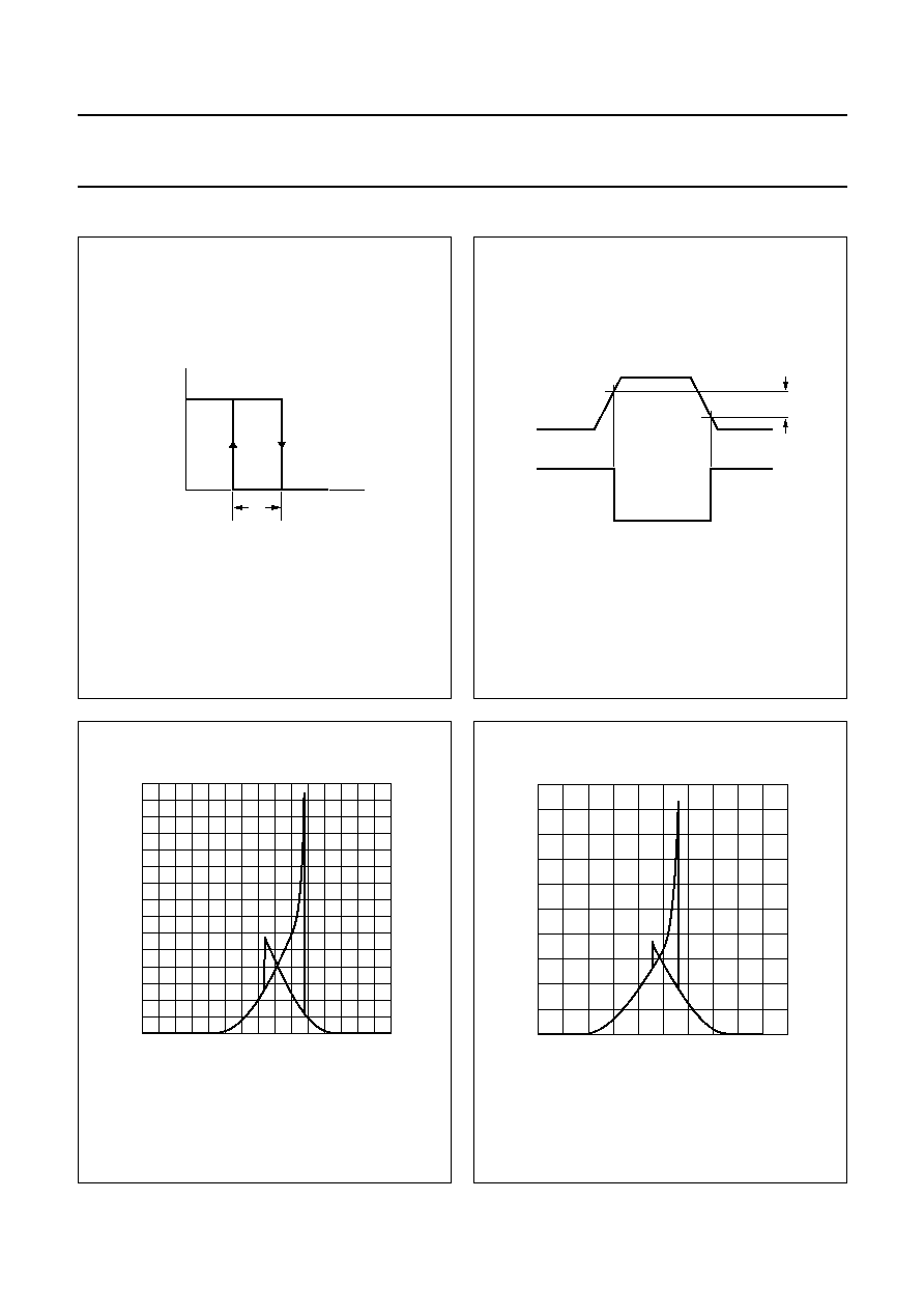
AC WAVEFORMS
Fig.6 The input (nA) to output (nY) propagation delays.
FAMILY
V
I
INPUT
REQUIREMENTS
V
M
INPUT
V
M
OUTPUT
74AHC14
GND to V
CC
0.5V
CC
0.5V
CC
74AHCT14
GND to 3.0 V
1.5 V
0.5V
CC
handbook, halfpage
MNA209
nA input
nY output
tPHL
tPLH
VM
VM
2003 May 26
14
Philips Semiconductors
Product specification
Hex inverting Schmitt trigger
74AHC14; 74AHCT14
Fig.7 Load circuitry for switching times.
handbook, full pagewidth
open
GND
VCC
VCC
VI
VO
MNA219
D.U.T.
CL
RT
RL =
1 k
PULSE
GENERATOR
S1
TEST
S1
t
PLH
/t
PHL
open
t
PLZ
/t
PZL
V
CC
t
PHZ
/t
PZH
GND
Definitions for test circuit:
R
L
= Load resistor.
C
L
= Load capacitance including jig and probe capacitance.
R
T
= Termination resistance should be equal to the output impedance Z
o
of the pulse generator.
2003 May 26
15
Philips Semiconductors
Product specification
Hex inverting Schmitt trigger
74AHC14; 74AHCT14
TRANSFER CHARACTERISTIC WAVEFORMS
Fig.8 Transfer characteristic.
MNA207
VO
VI
VH
VT
+
VT
-
Fig.9 The definition of V
T+
, V
T
-
and V
H
.
handbook, halfpage
MNA208
VO
VI
VH
VT
+
VT
-
V
T+
and V
T
-
are between limits of 20% and 70%.
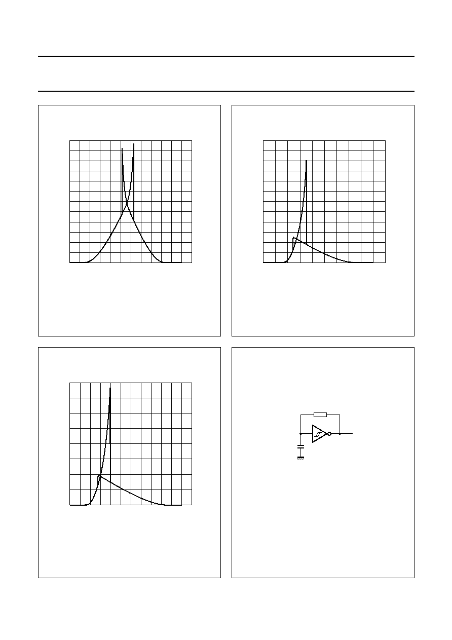
Fig.10 Typical 74AHC transfer characteristic.
handbook, halfpage
0
0
1
3
1.5
0.5
1
MNA411
2
VI (V)
ICC
(mA)
V
CC
= 3.0 V.
Fig.11 Typical 74AHC transfer characteristic.
handbook, halfpage
0
5
VI (V)
ICC
(mA)
5
0
1
MNA412
2
3
4
1
2
3
4
V
CC
= 4.5 V.
2003 May 26
16
Philips Semiconductors
Product specification
Hex inverting Schmitt trigger
74AHC14; 74AHCT14
Fig.12 Typical AHC transfer characteristic.
handbook, halfpage
0
2
6
6
0
2
4
MNA413
4
VI (V)
ICC
(mA)
V
CC
= 5.5 V.
Fig.13 Typical 74AHCT transfer characteristic.
handbook, halfpage
0
5
VI (V)
ICC
(mA)
6
0
MNA414
2
4
1
2
3
4
V
CC
= 4.5 V.
Fig.14 Typical 74AHCT transfer characteristics.
handbook, halfpage
0
2
6
8
0
2
4
6
MNA415
4
VI (V)
ICC
(mA)
V
CC
= 5.5 V.
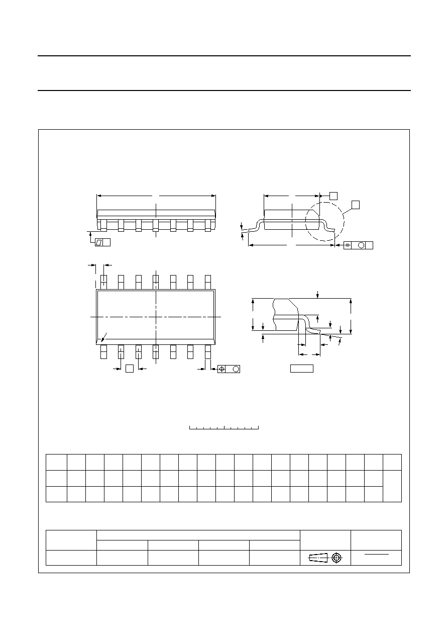
Fig.15 Relaxation oscillator.
handbook, halfpage
MNA206
R
C
74AHC14:
74AHCT14:
f
1
T
---
=
1
0.55RC
---------------------
f
1
T
---
=
1
0.60RC
---------------------
2003 May 26
17
Philips Semiconductors
Product specification
Hex inverting Schmitt trigger
74AHC14; 74AHCT14
PACKAGE OUTLINES
UNIT
A
max.
A
1
A
2
A
3
b
p
c
D
(1)
E
(1)
(1)
e
H
E
L
L
p
Q
Z
y
w
v
REFERENCES
OUTLINE
VERSION
EUROPEAN
PROJECTION
ISSUE DATE
IEC
JEDEC
JEITA
mm
inches
1.75
0.25
0.10
1.45
1.25
0.25
0.49
0.36
0.25
0.19
8.75
8.55
4.0
3.8
1.27
6.2
5.8
0.7
0.6
0.7
0.3
8
0
o
o
0.25
0.1
DIMENSIONS (inch dimensions are derived from the original mm dimensions)
Note
1. Plastic or metal protrusions of 0.15 mm (0.006 inch) maximum per side are not included.
1.0
0.4
SOT108-1
X
w
M
A
A
1
A
2
b
p
D
H
E
L
p
Q
detail X
E
Z
e
c
L
v
M
A
(A )
3
A
7
8
1
14
y
076E06
MS-012
pin 1 index
0.069
0.010
0.004
0.057
0.049
0.01
0.019
0.014
0.0100
0.0075
0.35
0.34
0.16
0.15
0.05
1.05
0.041
0.244
0.228
0.028
0.024
0.028
0.012
0.01
0.25
0.01
0.004
0.039
0.016
99-12-27
03-02-19
0
2.5
5 mm
scale
SO14: plastic small outline package; 14 leads; body width 3.9 mm
SOT108-1
2003 May 26
18
Philips Semiconductors
Product specification
Hex inverting Schmitt trigger
74AHC14; 74AHCT14
UNIT
A
1
A
2
A
3
b
p
c
D
(1)
E
(2)
(1)
e
H
E
L
L
p
Q
Z
y
w
v
REFERENCES
OUTLINE
VERSION
EUROPEAN
PROJECTION
ISSUE DATE
IEC
JEDEC
JEITA
mm
0.15
0.05
0.95
0.80
0.30
0.19
0.2
0.1
5.1
4.9
4.5
4.3
0.65
6.6
6.2
0.4
0.3
0.72
0.38
8
0
o
o
0.13
0.1
0.2
1
DIMENSIONS (mm are the original dimensions)
Notes
1. Plastic or metal protrusions of 0.15 mm maximum per side are not included.
2. Plastic interlead protrusions of 0.25 mm maximum per side are not included.
0.75
0.50
SOT402-1
MO-153
99-12-27
03-02-18
w
M
b
p
D
Z
e
0.25
1
7
14
8
A
A
1
A
2
L
p
Q
detail X
L
(A )
3
H
E
E
c
v
M
A
X
A
y
0
2.5
5 mm
scale
TSSOP14: plastic thin shrink small outline package; 14 leads; body width 4.4 mm
SOT402-1
A
max.
1.1
pin 1 index
2003 May 26
19
Philips Semiconductors
Product specification
Hex inverting Schmitt trigger
74AHC14; 74AHCT14
terminal 1
index area
0.5
1
A1
Eh
b
UNIT
y
e
0.2
c
REFERENCES
OUTLINE
VERSION
EUROPEAN
PROJECTION
ISSUE DATE
IEC
JEDEC
JEITA
mm
3.1
2.9
Dh
1.65
1.35
y1
2.6
2.4
1.15
0.85
e1
2
0.30
0.18
0.05
0.00
0.05
0.1
DIMENSIONS (mm are the original dimensions)
SOT762-1
MO-241
- - -
- - -
0.5
0.3
L
0.1
v
0.05
w
0
2.5
5 mm
scale
SOT762-1
DHVQFN14: plastic dual in-line compatible thermal enhanced very thin quad flat package; no leads;
14 terminals; body 2.5 x 3 x 0.85 mm
A
(1)
max.
A
A1
c
detail X
y
y1 C
e
L
Eh
Dh
e
e1
b
2
6
13
9
8
7
1
14
X
D
E
C
B
A
02-10-17
03-01-27
terminal 1
index area
A
C
C
B
v
M
w
M
E
(1)
Note
1. Plastic or metal protrusions of 0.075 mm maximum per side are not included.
D
(1)

2003 May 26
20
Philips Semiconductors
Product specification
Hex inverting Schmitt trigger
74AHC14; 74AHCT14
SOLDERING
Introduction to soldering surface mount packages
This text gives a very brief insight to a complex technology.
A more in-depth account of soldering ICs can be found in
our
"Data Handbook IC26; Integrated Circuit Packages"
(document order number 9398 652 90011).
There is no soldering method that is ideal for all surface
mount IC packages. Wave soldering can still be used for
certain surface mount ICs, but it is not suitable for fine pitch
SMDs. In these situations reflow soldering is
recommended.
Reflow soldering
Reflow soldering requires solder paste (a suspension of
fine solder particles, flux and binding agent) to be applied
to the printed-circuit board by screen printing, stencilling or
pressure-syringe dispensing before package placement.
Driven by legislation and environmental forces the
worldwide use of lead-free solder pastes is increasing.
Several methods exist for reflowing; for example,
convection or convection/infrared heating in a conveyor
type oven. Throughput times (preheating, soldering and
cooling) vary between 100 and 200 seconds depending
on heating method.
Typical reflow peak temperatures range from
215 to 270
°
C depending on solder paste material. The
top-surface temperature of the packages should
preferably be kept:
·
below 220
°
C (SnPb process) or below 245
°
C (Pb-free
process)
for all the BGA packages
for packages with a thickness
2.5 mm
for packages with a thickness < 2.5 mm and a
volume
350 mm
3
so called thick/large packages.
·
below 235
°
C (SnPb process) or below 260
°
C (Pb-free
process) for packages with a thickness < 2.5 mm and a
volume < 350 mm
3
so called small/thin packages.
Moisture sensitivity precautions, as indicated on packing,
must be respected at all times.
Wave soldering
Conventional single wave soldering is not recommended
for surface mount devices (SMDs) or printed-circuit boards
with a high component density, as solder bridging and
non-wetting can present major problems.
To overcome these problems the double-wave soldering
method was specifically developed.
If wave soldering is used the following conditions must be
observed for optimal results:
·
Use a double-wave soldering method comprising a
turbulent wave with high upward pressure followed by a
smooth laminar wave.
·
For packages with leads on two sides and a pitch (e):
larger than or equal to 1.27 mm, the footprint
longitudinal axis is preferred to be parallel to the
transport direction of the printed-circuit board;
smaller than 1.27 mm, the footprint longitudinal axis
must be parallel to the transport direction of the
printed-circuit board.
The footprint must incorporate solder thieves at the
downstream end.
·
For packages with leads on four sides, the footprint must
be placed at a 45
°
angle to the transport direction of the
printed-circuit board. The footprint must incorporate
solder thieves downstream and at the side corners.
During placement and before soldering, the package must
be fixed with a droplet of adhesive. The adhesive can be
applied by screen printing, pin transfer or syringe
dispensing. The package can be soldered after the
adhesive is cured.
Typical dwell time of the leads in the wave ranges from
3 to 4 seconds at 250
°
C or 265
°
C, depending on solder
material applied, SnPb or Pb-free respectively.
A mildly-activated flux will eliminate the need for removal
of corrosive residues in most applications.
Manual soldering
Fix the component by first soldering two
diagonally-opposite end leads. Use a low voltage (24 V or
less) soldering iron applied to the flat part of the lead.
Contact time must be limited to 10 seconds at up to
300
°
C.
When using a dedicated tool, all other leads can be
soldered in one operation within 2 to 5 seconds between
270 and 320
°
C.
2003 May 26
21
Philips Semiconductors
Product specification
Hex inverting Schmitt trigger
74AHC14; 74AHCT14
Suitability of surface mount IC packages for wave and reflow soldering methods
Notes
1. For more detailed information on the BGA packages refer to the
"(LF)BGA Application Note" (AN01026); order a copy
from your Philips Semiconductors sales office.
2. All surface mount (SMD) packages are moisture sensitive. Depending upon the moisture content, the maximum
temperature (with respect to time) and body size of the package, there is a risk that internal or external package
cracks may occur due to vaporization of the moisture in them (the so called popcorn effect). For details, refer to the
Drypack information in the
"Data Handbook IC26; Integrated Circuit Packages; Section: Packing Methods".
3. These packages are not suitable for wave soldering. On versions with the heatsink on the bottom side, the solder
cannot penetrate between the printed-circuit board and the heatsink. On versions with the heatsink on the top side,
the solder might be deposited on the heatsink surface.
4. If wave soldering is considered, then the package must be placed at a 45
°
angle to the solder wave direction.
The package footprint must incorporate solder thieves downstream and at the side corners.
5. Wave soldering is suitable for LQFP, TQFP and QFP packages with a pitch (e) larger than 0.8 mm; it is definitely not
suitable for packages with a pitch (e) equal to or smaller than 0.65 mm.
6. Wave soldering is suitable for SSOP, TSSOP, VSO and VSSOP packages with a pitch (e) equal to or larger than
0.65 mm; it is definitely not suitable for packages with a pitch (e) equal to or smaller than 0.5 mm.
PACKAGE
(1)
SOLDERING METHOD
WAVE
REFLOW
(2)
BGA, LBGA, LFBGA, SQFP, TFBGA, VFBGA
not suitable
suitable
DHVQFN, HBCC, HBGA, HLQFP, HSQFP, HSOP, HTQFP,
HTSSOP, HVQFN, HVSON, SMS
not suitable
(3)
suitable
PLCC
(4)
, SO, SOJ
suitable
suitable
LQFP, QFP, TQFP
not recommended
(4)(5)
suitable
SSOP, TSSOP, VSO, VSSOP
not recommended
(6)
suitable
2003 May 26
22
Philips Semiconductors
Product specification
Hex inverting Schmitt trigger
74AHC14; 74AHCT14
DATA SHEET STATUS
Notes
1. Please consult the most recently issued data sheet before initiating or completing a design.
2. The product status of the device(s) described in this data sheet may have changed since this data sheet was
published. The latest information is available on the Internet at URL http://www.semiconductors.philips.com.
3. For data sheets describing multiple type numbers, the highest-level product status determines the data sheet status.
LEVEL
DATA SHEET
STATUS
(1)
PRODUCT
STATUS
(2)(3)
DEFINITION
I
Objective data
Development
This data sheet contains data from the objective specification for product
development. Philips Semiconductors reserves the right to change the
specification in any manner without notice.
II
Preliminary data Qualification
This data sheet contains data from the preliminary specification.
Supplementary data will be published at a later date. Philips
Semiconductors reserves the right to change the specification without
notice, in order to improve the design and supply the best possible
product.
III
Product data
Production
This data sheet contains data from the product specification. Philips
Semiconductors reserves the right to make changes at any time in order
to improve the design, manufacturing and supply. Relevant changes will
be communicated via a Customer Product/Process Change Notification
(CPCN).
DEFINITIONS
Short-form specification
The data in a short-form
specification is extracted from a full data sheet with the
same type number and title. For detailed information see
the relevant data sheet or data handbook.
Limiting values definition
Limiting values given are in
accordance with the Absolute Maximum Rating System
(IEC 60134). Stress above one or more of the limiting
values may cause permanent damage to the device.
These are stress ratings only and operation of the device
at these or at any other conditions above those given in the
Characteristics sections of the specification is not implied.
Exposure to limiting values for extended periods may
affect device reliability.
Application information
Applications that are
described herein for any of these products are for
illustrative purposes only. Philips Semiconductors make
no representation or warranty that such applications will be
suitable for the specified use without further testing or
modification.
DISCLAIMERS
Life support applications
These products are not
designed for use in life support appliances, devices, or
systems where malfunction of these products can
reasonably be expected to result in personal injury. Philips
Semiconductors customers using or selling these products
for use in such applications do so at their own risk and
agree to fully indemnify Philips Semiconductors for any
damages resulting from such application.
Right to make changes
Philips Semiconductors
reserves the right to make changes in the products -
including circuits, standard cells, and/or software -
described or contained herein in order to improve design
and/or performance. When the product is in full production
(status `Production'), relevant changes will be
communicated via a Customer Product/Process Change
Notification (CPCN). Philips Semiconductors assumes no
responsibility or liability for the use of any of these
products, conveys no licence or title under any patent,
copyright, or mask work right to these products, and
makes no representations or warranties that these
products are free from patent, copyright, or mask work
right infringement, unless otherwise specified.

2003 May 26
23
Philips Semiconductors
Product specification
Hex inverting Schmitt trigger
74AHC14; 74AHCT14
NOTES

© Koninklijke Philips Electronics N.V. 2003
SCA75
All rights are reserved. Reproduction in whole or in part is prohibited without the prior written consent of the copyright owner.
The information presented in this document does not form part of any quotation or contract, is believed to be accurate and reliable and may be changed
without notice. No liability will be accepted by the publisher for any consequence of its use. Publication thereof does not convey nor imply any license
under patent- or other industrial or intellectual property rights.
Philips Semiconductors a worldwide company
Contact information
For additional information please visit http://www.semiconductors.philips.com.
Fax: +31 40 27 24825
For sales offices addresses send e-mail to: sales.addresses@www.semiconductors.philips.com.
Printed in The Netherlands
613508/03/pp
24
Date of release:
2003 May 26
Document order number:
9397 750 11221
Document Outline
- FEATURES
- DESCRIPTION
- QUICK REFERENCE DATA
- FUNCTION TABLE
- ORDERING INFORMATION
- PINNING
- RECOMMENDED OPERATING CONDITIONS
- LIMITING VALUES
- DC CHARACTERISTICS
- AC CHARACTERISTICS
- AC WAVEFORMS
- TRANSFER CHARACTERISTIC WAVEFORMS
- PACKAGE OUTLINES
- SOT108-1
- SOT402-1
- SOT762-1
- SOLDERING
- DATA SHEET STATUS
- DEFINITIONS
- DISCLAIMERS