Philips
Semiconductors
74ALS161B/74ALS163B
4-bit binary counter
Product specification
1991 Feb 08
INTEGRATED CIRCUITS
IC05 Data Handbook

Philips Semiconductors
Product specification
74ALS161B/74ALS163B
4-bit binary counter
74ALS161B
4-bit binary counter, asynchronous reset
74ALS163B
4-bit binary counter, synchronous reset
2
1991 Feb 08
853≠1350 01670
FEATURES
∑
Synchronous counting and loading
∑
Two count enable inputs for n-bit cascading
∑
Positive edge-triggered clock
∑
Asynchronous reset (74ALS161B)
∑
Synchronous reset (74ALS163B)
∑
High speed synchronous expansion
∑
Typical count rate of 140MHz
TYPE
TYPICAL f
MAX
TYPICAL
SUPPLY CURRENT
(TOTAL)
74ALS161B
140MHz
10mA
74ALS163B
140MHz
10mA
ORDERING INFORMATION
ORDER CODE
DESCRIPTION
COMMERCIAL RANGE
V
CC
= 5V
±
10%,
T
amb
= 0
∞
C to +70
∞
C
DRAWING
NUMBER
16-pin plastic DIP
74ALS161BN, 74ALS163BN
SOT38-4
16-pin plastic SO
74ALS161BD, 74ALS163BD
SOT109-1
16-pin plastic SSOP
Type II
74ALS161BDB,
74ALS163BDB
SOT338-1
DESCRIPTION
Synchronous presettable 4-bit binary counters (74ALS161B,
74ALS163B) feature an internal carry look-ahead and can be used
for high speed counting. Synchronous operation is provided by
having all flip-flops clocked simultaneously on the positive-going
edge of the clock. The clock input is buffered.
The outputs of the counters may be preset to High or Low level. A
Low level at the parallel enable (PE) input disables the counting
action and causes the data at the D0 ≠ D3 inputs to be loaded into
the counter on the positive-going edge of the clock (provided that
the setup and hold requirements for PE are met). Preset takes place
regardless of the levels at count enable (CEP, CET) inputs.
A Low level at the master reset (MR) input sets all the four outputs
of the flip-flops (Q0 ≠ Q3) in 74ALS161B to Low levels, regardless of
the levels at CP, PE, CET and CEP inputs (thus providing an
asynchronous clear function).
For the 74ALS163B the clear function is synchronous. A Low level
at the synchronous reset (SR) input sets all four outputs of the
flip-flops (Q0 ≠ Q3) to Low levels after the next positive-going
transition on the clock (CP) input ( provided that the setup and hold
time requirements for SR are met). This action occurs regardless of
the levels at CP, PE, CET and CEP inputs. The synchronous reset
feature enables the designer to modify the maximum count with only
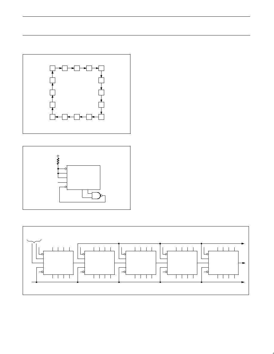
one external NAND gate (see Figure 1).
The carry look-ahead simplifies serial cascading of the counters.
Both count enable (CEP and CET) inputs must be High to count.
The CET input is fed forward to enable the TC output. The TC
output thus enabled will produce a High output pulse of a duration
approximately equal to the High level output of Q0. This pulse can
be used to enable the next cascaded stage (see Figure 2).
The TC output is subjected to decoding spikes due to internal race
conditions, Therefore, it is not recommended for use as clock or
asynchronous reset for flip-flops, registers, or counters.
INPUT AND OUTPUT LOADING AND FAN-OUT TABLE
PINS
DESCRIPTION
74ALS (U.L.)
HIGH/LOW
LOAD VALUE
HIGH/LOW
D0 ≠ D3
Data inputs
1.0/1.0
20
µ
A/0.1mA
CEP
Count enable parallel input (active-Low)
1.0/1.0
20
µ
A/0.1mA
CET
Count enable trickle input (active-Low)
1.0/1.0
20
µ
A/0.1mA
CP
Clock input (active rising edge)
1.0/1.0
20
µ
A/0.1mA
PE
Parallel enable input (active-Low)
1.0/1.0
20
µ
A/0.1mA
MR
Asynchronous master reset input (active-Low) for 74ALS161B
1.0/1.0
20
µ
A/0.1mA
SR
Asynchronous reset input (active-Low) for 74ALS163B
1.0/1.0
20
µ
A/0.1mA
Q0 ≠ Q3
Flip-flop outputs
20/80
0.4mA/8mA
TC
Terminal count output (active-Low)
20/80
0.4mA/8mA
NOTE:
One (1.0) ALS unit load is defined as: 20
µ
A in the High state and 0.1mA in the Low state.
Philips Semiconductors
Product specification
74ALS161B/74ALS163B
4-bit binary counter
1991 Feb 08
3
STATE DIAGRAM
8
7
6
5
4
12
11
10
9
13
14
15
0
1
2
3
SF00664
APPLICATIONS
Q0 Q1 Q2 Q3
CLOCK
PE
CEP
CET
CP
D1
D2
SC00086
D3
D0
SR
TC
74ALS163B
V
CC
Figure 1.
Maximum Count Modifying Scheme
Terminal Count = 6
Q0 Q1 Q2 Q3
PE
CEP
CET
CP
D1
D2
SC00087
D3
D0
SR
TC
Q0 Q1 Q2 Q3
PE
CEP
CET
CP
D1
D2 D3
D0
SR
TC
Q0 Q1 Q2 Q3
PE
CEP
CET
CP
D1
D2 D3
D0
SR
TC
Q0 Q1 Q2 Q3
PE
CEP
CET
CP
D1
D2 D3
D0
SR
TC
Q0 Q1 Q2 Q3
PE
CEP
CET
CP
D1
D2 D3
D0
SR
TC
74ALS163B
CP
H H = Enable count
or
L L = Disable count
74ALS163B
74ALS163B
74ALS163B
74ALS163B
Figure 2.
Synchronous Multistage Counting Scheme
Philips Semiconductors
Product specification
74ALS161B/74ALS163B
4-bit binary counter
1991 Feb 08
4
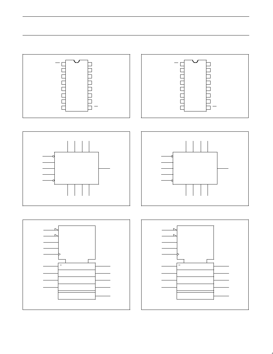
PIN CONFIGURATION ≠ 74ALS161B
16
15
14
13
12
11
10
7
6
5
4
3
2
1
CEP
V
CC
Q2
Q3
CET
Q1
TC
Q0
MR
CP
D3
D0
D1
D2
9
8
GND
PE
SF00656
PIN CONFIGURATION ≠ 74ALS163B
16
15
14
13
12
11
10
7
6
5
4
3
2
1
CEP
V
CC
Q2
Q3
CET
Q1
TC
Q0
SR
CP
D3
D0
D1
D2
9
8
GND
PE
SF00657
LOGIC SYMBOL ≠ 74ALS161B
Q0
Q1
Q2
Q3
14
13
12
11
V
CC
= Pin 16
GND = Pin 8
9
7
10
2
PE
CEP
CET
CP
D1
D2
5
6
SF00658
D3
D0
3
4
1
MR
TC
15
LOGIC SYMBOL ≠ 74ALS163B
Q0
Q1
Q2
Q3
14
13
12
11
V
CC
= Pin 16
GND = Pin 8
9
7
10
2
PE
CEP
CET
CP
D1
D2
5
6
SF00659
D3
D0
3
4
1
SR
TC
15
IEC/IEEE SYMBOL ≠ 74ALS161B
SF00660
3
1,2 D
1
9
M1
4
5
6
14
13
12
11
15
4 CT=15
7
G3
10
G4
2
C2 /1,3,4+
R
CTR DIV 16
IEC/IEEE SYMBOL ≠ 74ALS163B
SF00661
3
1,2 D
1
9
M1
4
5
6
14
13
12
11
15
4 CT=15
7
G3
10
G4
2
C2 /1,3,4+
2R
CTR DIV 16
Philips Semiconductors
Product specification
74ALS161B/74ALS163B
4-bit binary counter
1991 Feb 08
5
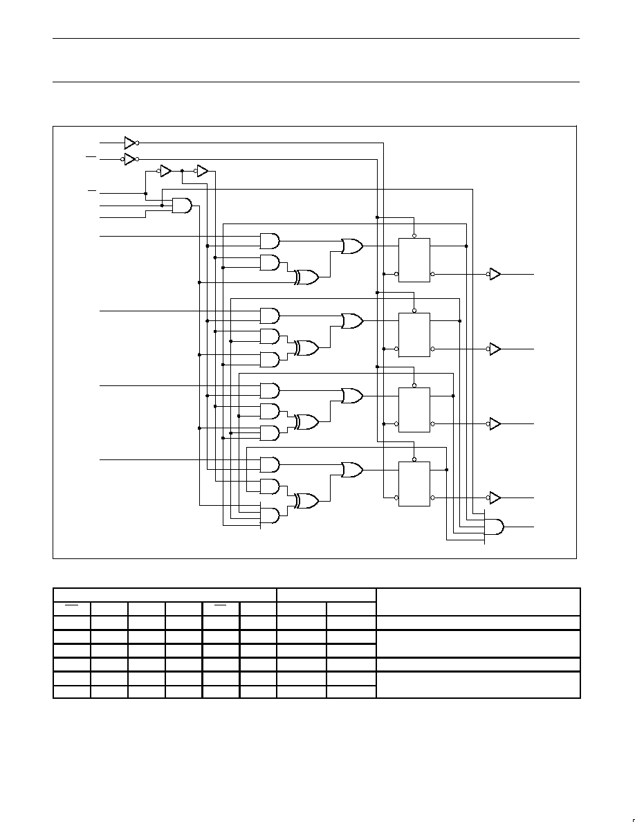
LOGIC DIAGRAM ≠ 74ALS161B
R
D
CP
Q
Q
R
D
CP
Q
Q
R
D
CP
Q
Q
R
D
CP
Q
Q
14
Q0
13
Q1
12
Q2
11
Q3
15
TC
6
D3
5
D2
4
D1
3
D0
7
CEP
10
CET
9
PE
1
MR
2
CP
SF00662
V
CC
= Pin 16
GND = Pin 8
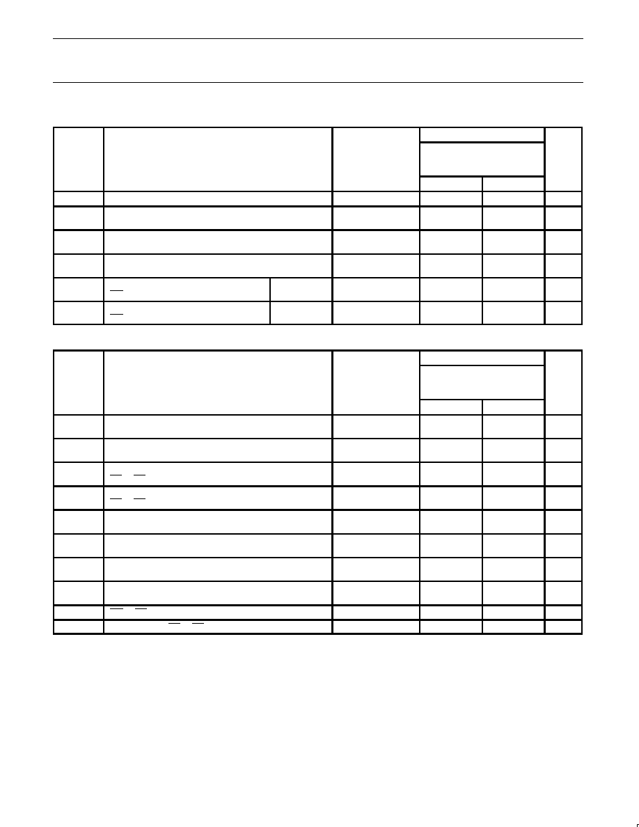
MODE SELECTION FUNCTION TABLE ≠ 74ALS161B
INPUTS
OUTPUTS
OPERATING MODE
MR
CP
CEP
CET
PE
Dn
Qn
TC
OPERATING MODE
L
X
X
X
X
X
L
L
Reset (clear)
H
X
X
l
l
L
L
Parallel load
H
X
X
l
h
H
(a)
Parallel load
H
h
h
h
X
count
(a)
Count
h
X
l
X
h
X
qn
(a)
Hold (do nothing)
h
X
X
l
h
X
qn
L
Hold (do nothing)
H = High-voltage level
h
= High state must be present one setup time before the Low-to-High clock transition
L
= Low-voltage level
l
= Low state must be present one setup time before the Low-to-High clock transition
qn = Lower case letters indicate the state of the referenced output prior to the Low-to-High clock transition
X = Don't care
(a) = The output is High when CET is High and the counter is at terminal count (HHHH)
= Low-to-High clock transition

Philips Semiconductors
Product specification
74ALS161B/74ALS163B
4-bit binary counter
1991 Feb 08
6
LOGIC DIAGRAM ≠ 74ALS163B
D
CP
Q
Q
D
CP
Q
Q
D
CP
Q
Q
D
CP
Q
Q
14
Q0
13
Q1
12
Q2
11
Q3
15
TC
6
D3
5
D2
4
D1
3
D0
7
CEP
10
CET
9
PE
1
SR
2
CP
SF00663
V
CC
= Pin 16
GND = Pin 8
MODE SELECTION FUNCTION TABLE ≠ 74ALS163B
INPUTS
OUTPUTS
OPERATING MODE
SR
CP
CEP
CET
PE
Dn
Qn
TC
OPERATING MODE
l
X
X
X
X
L
L
Reset (clear)
h
X
X
l
l
L
L
Parallel load
h
X
X
l
h
H
(a)
Parallel load
h
h
h
h
X
count
(a)
Count
h
X
l
X
h
X
qn
(a)
Hold (do nothing)
h
X
X
l
h
X
qn
L
Hold (do nothing)
H = High-voltage level
h
= High state must be present one setup time before the Low-to-High clock transition
L
= Low-voltage level
l
= Low state must be present one setup time before the Low-to-High clock transition
qn = Lower case letters indicate the state of the referenced output prior to the Low-to-High clock transition
X = Don't care
(a) = The output is High when CET is High and the counter is at terminal count (HHHH)
= Low-to-High clock transition
Philips Semiconductors
Product specification
74ALS161B/74ALS163B
4-bit binary counter
1991 Feb 08
7
ABSOLUTE MAXIMUM RATINGS
(Operation beyond the limit set forth in this table may impair the useful life of the device.
Unless otherwise noted these limits are over the operating free air temperature range.)
SYMBOL
PARAMETER
RATING
UNIT
V
CC
Supply voltage
≠0.5 to +7.0
V
V
IN
Input voltage
≠0.5 to +7.0
V
I
IN
Input current
≠30 to +5
mA
V
OUT
Voltage applied to output in High output state
≠0.5 to V
CC
V
I
OUT
Current applied to output in Low output state
16
mA
T
amb
Operating free-air temperature range
0 to +70
∞
C
T
stg
Storage temperature range
≠65 to +150
∞
C
RECOMMENDED OPERATING CONDITIONS
SYMBOL
PARAMETER
LIMITS
UNIT
SYMBOL
PARAMETER
MIN
NOM
MAX
UNIT
V
CC
Supply voltage
4.5
5.0
5.5
V
V
IH
High-level input voltage
2.0
V
V
IL
Low-level input voltage
0.8
V
I
IK
Input clamp current
≠18
mA
I
OH
High-level output current
≠0.4
mA
I
OL
Low-level output current
8
mA
T
amb
Operating free-air temperature range
0
+70
∞
C
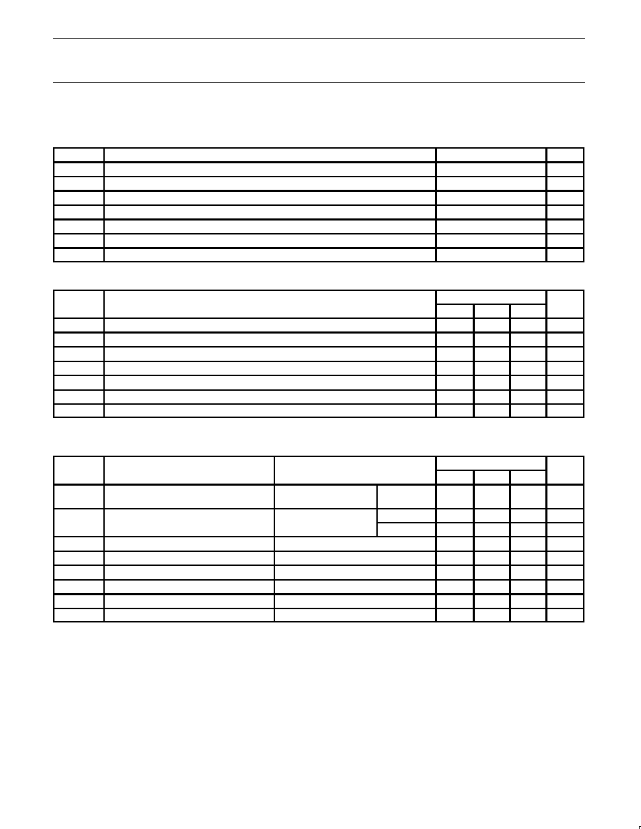
DC ELECTRICAL CHARACTERISTICS
(Over recommended operating free-air temperature range unless otherwise noted.)
SYMBOL
PARAMETER
TEST CONDITIONS
1
LIMITS
UNIT
SYMBOL
PARAMETER
TEST CONDITIONS
1
MIN
TYP
2
MAX
UNIT
V
O
High level output voltage
V
CC
=
±
10%, V
IL
= MAX,
I
O
= 0 4mA
V
CC
2
V
V
OH
High-level output voltage
CC
,
IL
,
V
IH
= MIN
I
OH
= ≠0.4mA
V
CC
≠ 2
V
V
O
Low level output voltage
V
CC
= MIN, V
IL
= MAX,
I
OL
= 4mA
0.25
0.40
V
V
OL
Low-level output voltage
CC
,
IL
,
V
IH
= MIN
I
OL
= 8mA
0.35
0.50
V
V
IK
Input clamp voltage
V
CC
= MIN, I
I
= I
IK
≠0.73
≠1.5
V
I
I
Input current at minimum input voltage
V
CC
= MAX, V
I
= 7.0V
0.1
mA
I
IH
High-level input current
V
CC
= MAX, V
I
= 2.7V
20
µ
A
I
IL
Low-level input current
V
CC
= MAX, V
I
= 0.4V
≠0.1
mA
I
O
Output current
3
V
CC
= MAX, V
O
= 2.25V
≠30
≠112
mA
I
CC
Supply current (total)
V
CC
= MAX
10
21
mA
NOTES:
1. For conditions shown as MIN or MAX, use the appropriate value specified under recommended operating conditions for the applicable type.
2. All typical values are at V
CC
= 5V, T
amb
= 25
∞
C.
3. The output conditions have been chosen to produce a current that closely approximates one half of the true short-circuit output current, I
OS
.
Philips Semiconductors
Product specification
74ALS161B/74ALS163B
4-bit binary counter
1991 Feb 08
8
AC ELECTRICAL CHARACTERISTICS
LIMITS
SYMBOL
PARAMETER
TEST CONDITION
T
amb
= 0
∞
C to +70
∞
C
V
CC
= +5.0V
±
10%
C
L
= 50pF, R
L
= 500
UNIT
MIN
MAX
f
MAX
Maximum clock frequency
Waveform 1
100
MHz
t
PLH
t
PHL
Propagation delay
CP to Qn
Waveform 1
4.0
6.0
13.0
16.0
ns
t
PLH
t
PHL
Propagation delay
CP to TC
Waveform 1
6.0
8.0
16.0
16.0
ns
t
PLH
t
PHL
Propagation delay
CET to TC
Waveform 2
3.0
3.0
10.0
10.0
ns
t
PHL
Propagation delay
MR to Qn
74ALS161B
Waveform 3
8.0
15.0
ns
t
PHL
Propagation delay
MR to TC
74ALS163B
Waveform 3
11.0
19.0
ns
AC ELECTRICAL CHARACTERISTICS
LIMITS
SYMBOL
PARAMETER
TEST CONDITION
T
amb
= 0
∞
C to +70
∞
C
V
CC
= +5.0V
±
10%
C
L
= 50pF, R
L
= 500
UNIT
MIN
MAX
t
su
(H)
t
su
(L)
Setup time, High or Low
Dn to CP
Waveform 6
8.0
8.0
ns
t
h
(H)
t
h
(L)
Hold time, High or Low
Dn to CP
Waveform 6
0.0
0.0
ns
t
su
(H)
t
su
(L)
Setup time, High or Low
PE or SR to CP
Waveform 5 or 6
10.0
10.0
ns
t
h
(H)
t
h
(L)
Hold time, High or Low
PE or SR to CP
Waveform 6
0.0
0.0
ns
t
su
(H)
t
su
(L)
Setup time, High or Low
CET or CEP to CP
Waveform 4
10.0
10.0
ns
t
h
(H)
t
h
(L)
Hold time, High or Low
CET or CEP to CP
Waveform 4
0.0
0.0
ns
t
w
(H)
t
w
(L)
CP Pulse width (load),
High or Low
Waveform 1
5.0
5.0
ns
t
w
(H)
t
w
(L)
CP Pulse width (count),
High or Low
Waveform 1
5.0
5.0
ns
t
w
(L)
MR or SR Pulse width, Low
Waveform 3
5.0
ns
t
REC
Recovery time, CR or SR to CP
Waveform 3
10.0
ns

Philips Semiconductors
Product specification
74ALS161B/74ALS163B
4-bit binary counter
1991 Feb 08
9
AC WAVEFORMS
For all waveforms, V
M
= 1.3V.
The shaded areas indicate when the input is permitted to change for predictable output performance.
V
M
SC00088
V
M
V
M
V
M
V
M
1/f
MAX
t
w
(H)
t
w
(L)
t
PLH
t
PHL
CP
Qn, TC
Waveform 1.
Propagation Delay for Clock Input to Output,
Clock PUlse Width, and Maximum Clock Frequency
V
M
SF00668
V
M
V
M
t
PLH
CET
TC
V
M
t
PHL
Waveform 2.
Propagation Delay for CET to TC Output
SF00669
MR
CP
V
M
V
M
V
M
V
M
t
w
(L)
t
PHL
t
REC
Qn, TC
Waveform 3.
Master Reset Pulse Width,
Master Reset to Output Delay,
and Master Reset to Clock Recovery Time
SC00089
V
M
V
M
V
M
V
M
V
M
V
M
t
su
(H)
t
su
(L)
t
h
(H)
t
h
(L)
CEP
CET
CP
Waveform 4.
CEP and CET Setup and Hold Times
SC00090
V
M
V
M
V
M
V
M
V
M
V
M
t
su
(L)
t
su
(H)
t
h
(L)
t
h
(H)
SR
CP
Waveform 5.
Synchronous Reset Setup and Hold Times
SC00091
V
M
V
M
V
M
V
M
V
M
V
M
t
su
(L)
t
su
(H)
t
h
(L)
t
h
(H)
PE
CP
V
M
V
M
Dn
t
su
t
h
Waveform 6.
Data and Parallel Enable Setup and Hold Times

Philips Semiconductors
Product specification
74ALS161B/74ALS163B
4-bit binary counter
1991 Feb 08
10
TEST CIRCUIT AND WAVEFORMS
tw
90%
VM
10%
90%
VM
10%
90%
VM
10%
90%
VM
10%
NEGATIVE
PULSE
POSITIVE
PULSE
tw
AMP (V)
0.3V
0.3V
tTHL (tf
f
)
INPUT PULSE REQUIREMENTS
Rep.Rate
t
w
t
TLH
t
THL
1MHz
500ns
2.0ns
2.0ns
Input Pulse Definition
VCC
Family
74ALS
D.U.T.
PULSE
GENERATOR
RL
CL
RT
VIN
VOUT
Test Circuit for Totem-pole Outputs
DEFINITIONS:
R
L
= Load resistor;
see AC electrical characteristics for value.
C
L
= Load capacitance includes jig and probe capacitance;
see AC electrical characteristics for value.
R
T
= Termination resistance should be equal to Z
OUT
of
pulse generators.
tTHL (tf
)
tTLH (tr
)
tTLH (tr
)
AMP (V)
Amplitude
3.5V
1.3V
V
M
SC00005
Philips Semiconductors
Product specification
74ALS161B
74ALS163B
4-bit binary counter
1991 Feb 08
11
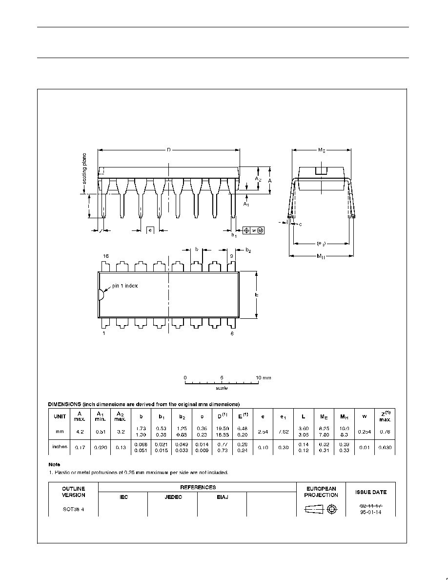
DIP16:
plastic dual in-line package; 16 leads (300 mil)
SOT38-4
Philips Semiconductors
Product specification
74ALS161B
74ALS163B
4-bit binary counter
1991 Feb 08
12
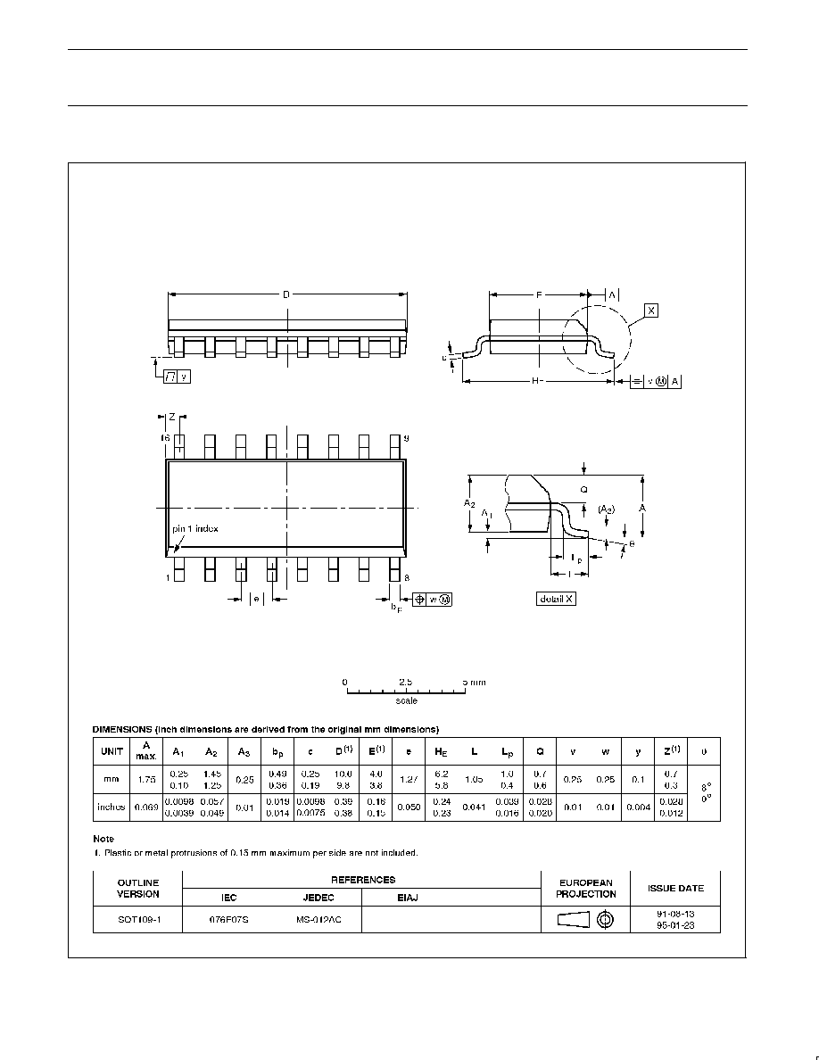
SO16:
plastic small outline package; 16 leads; body width 3.9 mm
SOT109-1
Philips Semiconductors
Product specification
74ALS161B
74ALS163B
4-bit binary counter
1991 Feb 08
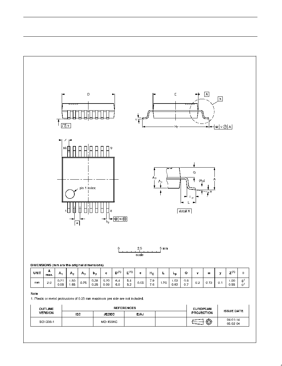
13
SSOP16:
plastic shrink small outline package; 16 leads; body width 5.3 mm
SOT338-1
Philips Semiconductors
Product specification
74ALS161B
74ALS163B
4-bit binary counter
1991 Feb 08
14
Philips Semiconductors and Philips Electronics North America Corporation reserve the right to make changes, without notice, in the products,
including circuits, standard cells, and/or software, described or contained herein in order to improve design and/or performance. Philips
Semiconductors assumes no responsibility or liability for the use of any of these products, conveys no license or title under any patent, copyright,
or mask work right to these products, and makes no representations or warranties that these products are free from patent, copyright, or mask
work right infringement, unless otherwise specified. Applications that are described herein for any of these products are for illustrative purposes
only. Philips Semiconductors makes no representation or warranty that such applications will be suitable for the specified use without further testing
or modification.
LIFE SUPPORT APPLICATIONS
Philips Semiconductors and Philips Electronics North America Corporation Products are not designed for use in life support appliances, devices,
or systems where malfunction of a Philips Semiconductors and Philips Electronics North America Corporation Product can reasonably be expected
to result in a personal injury. Philips Semiconductors and Philips Electronics North America Corporation customers using or selling Philips
Semiconductors and Philips Electronics North America Corporation Products for use in such applications do so at their own risk and agree to fully
indemnify Philips Semiconductors and Philips Electronics North America Corporation for any damages resulting from such improper use or sale.
This data sheet contains preliminary data, and supplementary data will be published at a later date. Philips
Semiconductors reserves the right to make changes at any time without notice in order to improve design
and supply the best possible product.
Philips Semiconductors
811 East Arques Avenue
P.O. Box 3409
Sunnyvale, California 94088≠3409
Telephone 800-234-7381
DEFINITIONS
Data Sheet Identification
Product Status
Definition
Objective Specification
Preliminary Specification
Product Specification
Formative or in Design
Preproduction Product
Full Production
This data sheet contains the design target or goal specifications for product development. Specifications
may change in any manner without notice.
This data sheet contains Final Specifications. Philips Semiconductors reserves the right to make changes
at any time without notice, in order to improve design and supply the best possible product.
©
Copyright Philips Electronics North America Corporation 1997
All rights reserved. Printed in U.S.A.
Philips
Semiconductors