 | –≠–ª–µ–∫—Ç—Ä–æ–Ω–Ω—ã–π –∫–æ–º–ø–æ–Ω–µ–Ω—Ç: 74ALS623A | –°–∫–∞—á–∞—Ç—å:  PDF PDF  ZIP ZIP |
Document Outline
- FEATURES
- ORDERING INFORMATION
- DESCRIPTION
- INPUT AND OUTPUT LOADING AND FAN-OUT TABLE
- PIN CONFIGURATION Ö 74ALS620A/74ALS620A-1
- PIN CONFIGURATION Ö 74ALS623A/74ALS623A-1
- LOGIC SYMBOL Ö 74ALS620A/74ALS620A-1
- LOGIC SYMBOL Ö 74ALS623A/74ALS623A-1
- IEC/IEEE SYMBOL Ö 74ALS620A/74ALS620A-1
- IEC/IEEE SYMBOL Ö 74ALS623A/74ALS623A-1
- LOGIC DIAGRAM Ö 74ALS620A/74ALS620A-1
- LOGIC DIAGRAM Ö 74ALS623A/74ALS623A-1
- FUNCTION TABLE
- ABSOLUTE MAXIMUM RATINGS
- RECOMMENDED OPERATING CONDITIONS
- DC ELECTRICAL CHARACTERISTICS
- AC ELECTRICAL CHARACTERISTICS FOR 74ALS620A/74ALS620A-1
- AC ELECTRICAL CHARACTERISTICS FOR 74ALS623A/74ALS623A-1
- AC WAVEFORMS
- TEST CIRCUIT AND WAVEFORMS
- PACKAGE OUTLINES
- DEFINITIONS

Philips
Semiconductors
74ALS620A/74ALS620A≠1
74ALS623A/74ALS623A≠1
Transceivers
Product specification
IC05 Data Handbook
1991 Feb 08
INTEGRATED CIRCUITS

Philips Semiconductors
Product specification
74ALS620A/74ALS620A-1
74ALS623A/74ALS623A-1
Transceivers
74ALS620A/74ALS620A-1 Octal bus transceiver, inverting (3-State)
74ALS623A/74ALS623A-1 Octal bus transceiver, non-inverting (3-State)
2
1991 Feb 08
853≠0020 01670
FEATURES
∑
Octal bidirectional bus interface
∑
3-State buffer outputs sink 24mA and source 15mA
∑
The -1 version sinks 48mA I
OL
within the +5% V
CC
range
TYPE
TYPICAL
PROPAGATION
DELAY
TYPICAL
SUPPLY CURRENT
(TOTAL)
74ALS620A/620A-1
4.0ns
33mA
74ALS623A/623A-1
4.0ns
38mA
ORDERING INFORMATION
ORDER CODE
DESCRIPTION
COMMERCIAL RANGE
V
CC
= 5V
±
10%,
T
amb
= 0
∞
C to +70
∞
C
DRAWING
NUMBER
20-pin plastic DIP
74ALS620AN, 74ALS620A-1N
74ALS623AN, 74ALS623A-1N
SOT146-1
20-pin plastic SOL
74ALS620AD, 74ALS620A-1D
74ALS623AD, 74ALS623A-1D
SOT163-1
DESCRIPTION
The 74ALS620A and 74ALS623A are octal transceiver featuring
3-State bus compatible outputs in both transmit and receive
directions. The 74ALS620A is an inverting version of the
74ALS623A. The outputs are capable of sinking 24mA and sourcing
up to 15mA, providing very good capacitive drive characteristics.
The outputs for the 74ALS620A-1 and 74ALS623A are capable of
sinking up to 48mA when within the
±
5% V
CC
range.
These octal bus transceivers are designed for asynchronous
two-way communication between data buses. The control function
implementation allows for maximum flexibility in timing.
These devices allow data transmission from the A bus to the B bus
or from B bus to A bus, depending on the logic levels at the enable
inputs (OEBA and OEAB). The enable inputs can be used to disable
the device so that the buses are effectively isolated. The
dual-enable configuration gives the 74ALS620A and 74ALS623A the
capability to store data by the simultaneous enabling of OEBA and
OEAB. Each output reinforces its input in this transceiver
configuration. Thus when both control inputs are enabled and all
other data sources to the two sets of the bus lines are at high
impedance, both sets of the bus lines (16 in all) will remain at their
last states.
INPUT AND OUTPUT LOADING AND FAN-OUT TABLE
PINS
DESCRIPTION
74ALS (U.L.)
HIGH/LOW
LOAD VALUE
HIGH/LOW
A0 ≠ A7, B0 ≠ B7
Data inputs
1.0/1.0
20
µ
A/0.1mA
OEBA, OEAB
Output Enable inputs
1.0/1.0
20
µ
A/0.1mA
A0 ≠ A7, B0 ≠ B7
Data outputs
750/240
15mA/24mA
A0 ≠ A7, B0 ≠ B7
Data outputs (-1 version)
750/480
15mA/48mA
NOTE:
One (1.0) ALS unit load is defined as: 20
µ
A in the High state and 0.1mA in the Low state.
PIN CONFIGURATION ≠ 74ALS620A/74ALS620A-1
1
2
3
4
5
6
7
8
9
10
11
12
13
14
15
16
17
18
19
20
OEAB
A0
A1
A2
A3
A4
A5
A6
A7
GND
V
CC
OEBA
B0
B1
B2
B3
B4
B6
B5
B7
SC00101
PIN CONFIGURATION ≠ 74ALS623A/74ALS623A-1
1
2
3
4
5
6
7
8
9
10
11
12
13
14
15
16
17
18
19
20
OEAB
A0
A1
A2
A3
A4
A5
A6
A7
GND
V
CC
OEBA
B0
B1
B2
B3
B4
B6
B5
B7
SC00102

Philips Semiconductors
Product specification
74ALS620A/74ALS620A-1
74ALS623A/74ALS623A-1
Transceivers
1991 Feb 08
3
LOGIC SYMBOL ≠ 74ALS620A/74ALS620A-1
SC00103
V
CC
= Pin 20
GND = Pin 10
2
3
4
5
6
7
8
9
A0
A1
A2
A3
A4
A5
A6
A7
B0
B1
B2
B3
B4
B5
B6
B7
18
17
16
15
14
13
12
11
1
19
OEAB
OEBA
LOGIC SYMBOL ≠ 74ALS623A/74ALS623A-1
SC00104
V
CC
= Pin 20
GND = Pin 10
2
3
4
5
6
7
8
9
A0
A1
A2
A3
A4
A5
A6
A7
B0
B1
B2
B3
B4
B5
B6
B7
18
17
16
15
14
13
12
11
1
19
OEAB
OEBA
IEC/IEEE SYMBOL ≠ 74ALS620A/74ALS620A-1
SC00105
9
11
8
12
7
13
6
14
5
15
4
16
3
17
2
18
19
1
2
1
EN1
EN2
IEC/IEEE SYMBOL ≠ 74ALS623A/74ALS623A-1
SC00106
9
11
8
12
7
13
6
14
5
15
4
16
3
17
2
18
19
1
2
1
EN1
EN2

Philips Semiconductors
Product specification
74ALS620A/74ALS620A-1
74ALS623A/74ALS623A-1
Transceivers
1991 Feb 08
4
LOGIC DIAGRAM ≠ 74ALS620A/74ALS620A-1
19
1
2
OEBA
OEAB
A0
18
B0
3
A1
17
B1
4
A2
16
B2
5
A3
15
B3
6
A4
14
B4
7
A5
13
B5
8
A6
12
B6
9
A7
11
B7
V
CC
= Pin 20
GND = Pin 10
SC00107
LOGIC DIAGRAM ≠ 74ALS623A/74ALS623A-1
19
1
2
OEBA
OEAB
A0
18
B0
3
A1
17
B1
4
A2
16
B2
5
A3
15
B3
6
A4
14
B4
7
A5
13
B5
8
A6
12
B6
9
A7
11
B7
V
CC
= Pin 20
GND = Pin 10
SC00108
FUNCTION TABLE
INPUTS
OPERATING MODES
OEBA
OEAB
74ALS620A
74ALS623A
L
L
B data to A Bus
B data to A Bus
L
H
A data to B Bus
A data to B Bus
H
L
Z
Z
L
H
B data to A Bus
B data to A Bus
L
H
A data to B Bus
A data to B Bus
H = High voltage level
L
= Low voltage level
X = Don't care
Z = High impedance "off" state

Philips Semiconductors
Product specification
74ALS620A/74ALS620A-1
74ALS623A/74ALS623A-1
Transceivers
1991 Feb 08
5
ABSOLUTE MAXIMUM RATINGS
(Operation beyond the limit set forth in this table may impair the useful life of the device.
Unless otherwise noted these limits are over the operating free air temperature range.)
SYMBOL
PARAMETER
RATING
UNIT
V
CC
Supply voltage
≠0.5 to +7.0
V
V
IN
Input voltage
≠0.5 to +7.0
V
I
IN
Input current
≠30 to +5
mA
V
OUT
Voltage applied to output in High output state
≠0.5 to V
CC
V
I
O
Current applied to output in Low output state
All versions
48
mA
I
OUT
Current applied to output in Low output state
-1 version
96
mA
T
amb
Operating free-air temperature range
0 to +70
∞
C
T
stg
Storage temperature range
≠65 to +150
∞
C
RECOMMENDED OPERATING CONDITIONS
SYMBOL
PARAMETER
LIMITS
UNIT
SYMBOL
MIN
NOM
MAX
UNIT
V
CC
Supply voltage
4.5
5.0
5.5
V
V
IH
High-level input voltage
2.0
V
V
IL
Low-level input voltage
0.8
V
I
IK
Input clamp current
≠18
mA
I
OH
High-level output current
≠15
mA
I
O
Low level output current
All versions
24
mA
I
OL
Low-level output current
-1 version
48
1
mA
T
amb
Operating free-air temperature range
0
+70
∞
C
NOTE:
1. The 48mA limit applies only under the condition of V
CC
= 5.0V
±
5%.

Philips Semiconductors
Product specification
74ALS620A/74ALS620A-1
74ALS623A/74ALS623A-1
Transceivers
1991 Feb 08
6
DC ELECTRICAL CHARACTERISTICS
(Over recommended operating free-air temperature range unless otherwise noted.)
SYMBOL
PARAMETER
TEST CONDITIONS
1
LIMITS
UNIT
SYMBOL
PARAMETER
TEST CONDITIONS
1
MIN
TYP
2
MAX
UNIT
V
CC
=
±
10%, V
IL
= MAX,
I
OH
= ≠0.4mA
V
CC
≠ 2
V
V
OH
High-level output voltage
CC
,
IL
,
V
IH
= MIN
I
OH
= ≠3mA
2.4
3.2
V
V
OH
High level out ut voltage
V
CC
= MIN, V
IL
= MAX,
V
IH
= MIN
I
OH
= ≠15mA
2.0
V
All versions
V
CC
= MIN, V
IL
= MAX,
I
OL
= 12mA
0.25
0.40
V
V
OL
Low-level output
voltage
All versions
CC
,
IL
,
V
IH
= MIN
I
OL
= 24mA
0.35
0.50
V
V
OL
voltage
≠1 versions
V
CC
= 4.75V, V
IL
= MAX,
V
IH
= MIN
I
OL
= 48mA
0.35
0.50
V
V
IK
Input clamp voltage
V
CC
= MIN, I
I
= I
IK
≠0.73
≠1.5
V
I
Input current at
maximum input
OEBA or OEAB
V
CC
= MAX, V
I
= 7.0V
0.1
mA
I
I
maximum in ut
voltage
A or B ports
V
CC
= MAX, V
I
= 5.5V
0.1
mA
I
IH
High-level input current
3
V
CC
= MAX, V
I
= 2.7V
20
µ
A
I
IL
Low-level input current
3
V
CC
= MAX, V
I
= 0.4V
≠0.1
mA
I
O
Output current
4
V
CC
= MAX, V
O
= 2.25V
≠30
≠112
mA
S
I
CCH
24
34
mA
74ALS620A
74ALS620A-1
I
CCL
V
CC
= MAX
42
49
mA
I
CC
Supply current (total)
74ALS620A 1
I
CCZ
45
52
mA
I
CC
Supply current (total)
I
CCH
24
43
mA
74ALS623A
74ALS623A-1
I
CCL
V
CC
= MAX
41
50
mA
74ALS623A 1
I
CCZ
46
55
mA
NOTES:
1. For conditions shown as MIN or MAX, use the appropriate value specified under recommended operating conditions for the applicable type.
2. All typical values are at V
CC
= 5V, T
amb
= 25
∞
C.
3. For I/O ports, the parameter I
IH
and I
IL
include the off-state current.
4. The output conditions have been chosen to produce a current that closely approximates one half of the true short-circuit output current, I
OS
.

Philips Semiconductors
Product specification
74ALS620A/74ALS620A-1
74ALS623A/74ALS623A-1
Transceivers
1991 Feb 08
7
AC ELECTRICAL CHARACTERISTICS FOR 74ALS620A/74ALS620A-1
LIMITS
SYMBOL
PARAMETER
TEST CONDITION
T
amb
= 0
∞
C to +70
∞
C
V
CC
= +5.0V
±
10%
C
L
= 50pF, R
L
= 500
UNIT
MIN
MAX
t
PLH
t
PHL
Propagation delay
An to Bn, Bn to An
Waveform 1
2.0
2.0
10.0
10.0
ns
t
PZH
t
PZL
Output enable time
OEBA to An
Waveform 3
Waveform 4
2.0
3.0
17.0
25.0
ns
t
PHZ
t
PLZ
Output disable time
OEBA to An
Waveform 3
Waveform 4
2.0
2.0
12.0
18.0
ns
t
PZH
t
PZL
Output enable time
OEAB to Bn
Waveform 3
Waveform 4
2.0
3.0
18.0
25.0
ns
t
PHZ
t
PLZ
Output disable time
OEAB to Bn
Waveform 3
Waveform 4
2.0
3.0
12.0
18.0
ns
AC ELECTRICAL CHARACTERISTICS FOR 74ALS623A/74ALS623A-1
LIMITS
SYMBOL
PARAMETER
TEST CONDITION
T
amb
= 0
∞
C to +70
∞
C
V
CC
= +5.0V
±
10%
C
L
= 50pF, R
L
= 500
UNIT
MIN
MAX
t
PLH
t
PHL
Propagation delay
An to Bn, Bn to An
Waveform 2
2.0
2.0
13.0
11.0
ns
t
PZH
t
PZL
Output enable time
OEBA to An
Waveform 3
Waveform 4
2.0
3.0
22.0
22.0
ns
t
PHZ
t
PLZ
Output disable time
OEBA to An
Waveform 3
Waveform 4
2.0
2.0
16.0
19.0
ns
t
PZH
t
PZL
Output enable time
OEAB to Bn
Waveform 3
Waveform 4
2.0
3.0
22.0
22.0
ns
t
PHZ
t
PLZ
Output disable time
OEAB to Bn
Waveform 3
Waveform 4
2.0
2.0
16.0
19.0
ns

Philips Semiconductors
Product specification
74ALS620A/74ALS620A-1
74ALS623A/74ALS623A-1
Transceivers
1991 Feb 08
8
AC WAVEFORMS
For all waveforms, V
M
= 1.3V.
An, Bn
Bn, An
tPHL
VM
VM
VM
VM
tPLH
SF00773
Waveform 1.
Propagation Delay for Inverting Outputs
V
M
V
M
V
M
V
M
Bn, An
An, Bn
t
PLH
t
PHL
SF00202
Waveform 2.
Propagation Delay for Non-inverting Outputs
SF00412
VM
VM
VM
tPHZ
tPZH
VOH -0.3V
0V
An or Bn
OEBA
OEAB
Waveform 3.
3-State Output Enable Time to High Level
and Disable Time from High Level
SF00413
VM
VM
VM
tPLZ
tPZL
VOL +0.3V
An or Bn
OEBA
OEAB
Waveform 4.
3-State Output Enable Time to Low Level
and Disable Time from Low Level
TEST CIRCUIT AND WAVEFORMS
tw
90%
VM
10%
90%
VM
10%
90%
VM
10%
90%
VM
10%
NEGATIVE
PULSE
POSITIVE
PULSE
tw
AMP (V)
0.3V
0.3V
tTHL (tf
f
)
INPUT PULSE REQUIREMENTS
Rep.Rate
t
w
t
TLH
t
THL
1MHz
500ns
2.0ns
2.0ns
Input Pulse Definition
VCC
Family
74ALS
D.U.T.
PULSE
GENERATOR
RL
CL
RT
VIN
VOUT
Test Circuit for 3-State Outputs
DEFINITIONS:
R
L
= Load resistor;
see AC electrical characteristics for value.
C
L
= Load capacitance includes jig and probe capacitance;
see AC electrical characteristics for value.
R
T
= Termination resistance should be equal to Z
OUT
of
pulse generators.
tTHL (tf
)
tTLH (tr
)
tTLH (tr
)
AMP (V)
Amplitude
3.5V
1.3V
V
M
SC00072
RL
7.0V
SWITCH POSITION
TEST
SWITCH
t
PLZ
, t
PZL
closed
All other
open
Transceivers
Philips Semiconductors
Product specification
74ALS620A/74ALS620A≠1
74ALS623A/74ALS623A≠1
1991 Feb 08
9
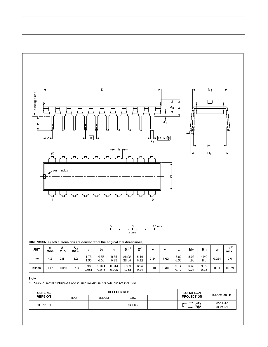
DIP20:
plastic dual in-line package; 20 leads (300 mil)
SOT146-1

Transceivers
Philips Semiconductors
Product specification
74ALS620A/74ALS620A≠1
74ALS623A/74ALS623A≠1
1991 Feb 08
10
SO20:
plastic small outline package; 20 leads; body width 7.5 mm
SOT163-1

Transceivers
Philips Semiconductors
Product specification
74ALS620A/74ALS620A≠1
74ALS623A/74ALS623A≠1
1991 Feb 08
11
Philips Semiconductors and Philips Electronics North America Corporation reserve the right to make changes, without notice, in the products,
including circuits, standard cells, and/or software, described or contained herein in order to improve design and/or performance. Philips
Semiconductors assumes no responsibility or liability for the use of any of these products, conveys no license or title under any patent, copyright,
or mask work right to these products, and makes no representations or warranties that these products are free from patent, copyright, or mask
work right infringement, unless otherwise specified. Applications that are described herein for any of these products are for illustrative purposes
only. Philips Semiconductors makes no representation or warranty that such applications will be suitable for the specified use without further testing
or modification.
LIFE SUPPORT APPLICATIONS
Philips Semiconductors and Philips Electronics North America Corporation Products are not designed for use in life support appliances, devices,
or systems where malfunction of a Philips Semiconductors and Philips Electronics North America Corporation Product can reasonably be expected
to result in a personal injury. Philips Semiconductors and Philips Electronics North America Corporation customers using or selling Philips
Semiconductors and Philips Electronics North America Corporation Products for use in such applications do so at their own risk and agree to fully
indemnify Philips Semiconductors and Philips Electronics North America Corporation for any damages resulting from such improper use or sale.
This data sheet contains preliminary data, and supplementary data will be published at a later date. Philips
Semiconductors reserves the right to make changes at any time without notice in order to improve design
and supply the best possible product.
Philips Semiconductors
811 East Arques Avenue
P.O. Box 3409
Sunnyvale, California 94088≠3409
Telephone 800-234-7381
DEFINITIONS
Data Sheet Identification
Product Status
Definition
Objective Specification
Preliminary Specification
Product Specification
Formative or in Design
Preproduction Product
Full Production
This data sheet contains the design target or goal specifications for product development. Specifications
may change in any manner without notice.
This data sheet contains Final Specifications. Philips Semiconductors reserves the right to make changes
at any time without notice, in order to improve design and supply the best possible product.
©
Copyright Philips Electronics North America Corporation 1997
All rights reserved. Printed in U.S.A.
Philips
Semiconductors