 | –≠–ª–µ–∫—Ç—Ä–æ–Ω–Ω—ã–π –∫–æ–º–ø–æ–Ω–µ–Ω—Ç: 74ALVC14 | –°–∫–∞—á–∞—Ç—å:  PDF PDF  ZIP ZIP |
1.
General description
The 74ALVC14 is a high-performance, low-power, low-voltage, Si-gate CMOS device and
superior to most advanced CMOS compatible TTL families.
The 74ALVC14 provides six inverting buffers with Schmitt-trigger action. It is capable of
transforming slowly changing input signals into sharply defined, jitter-free output signals.
2.
Features
s
Wide supply voltage range from 1.65 V to 3.6 V
s
3.6 V tolerant inputs/outputs
s
CMOS low power consumption
s
Direct interface with TTL levels (2.7 V to 3.6 V)
s
Power-down mode
s
Unlimited input rise and fall times
s
Latch-up performance exceeds 250 mA
s
Complies with JEDEC standard:
x
JESD8-7 (1.65 V to 1.95 V)
x
JESD8-5 (2.3 V to 2.7 V)
x
JESD8-B/JESD36 (2.7 V to 3.6 V)
s
ESD protection:
x
HBM EIA/JESD22-A114-B exceeds 2000 V
x
MM EIA/JESD22-A115-A exceeds 200 V
s
Multiple package options
3.
Quick reference data
74ALVC14
Hex inverting Schmitt trigger
Rev. 03 -- 15 February 2005
Product data sheet
Table 1:
Quick reference data
Symbol
Parameter
Conditions
Min
Typ
Max
Unit
t
PHL
, t
PLH
propagation delay nA
to nY
V
CC
= 1.8 V; C
L
= 30 pF;
R
L
= 1 k
-
2.9
-
ns
V
CC
= 2.5 V; C
L
= 30 pF;
R
L
= 500
-
2.2
-
ns
V
CC
= 2.7 V; C
L
= 50 pF;
R
L
= 500
-
2.8
-
ns
V
CC
= 3.3 V; C
L
= 50 pF;
R
L
= 500
-
2.4
-
ns
9397 750 14592
© Koninklijke Philips Electronics N.V. 2005. All rights reserved.
Product data sheet
Rev. 03 -- 15 February 2005
2 of 16
Philips Semiconductors
74ALVC14
Hex inverting Schmitt trigger
[1]
C
PD
is used to determine the dynamic power dissipation (P
D
in
µ
W).
P
D
= C
PD
◊
V
CC
2
◊
f
i
◊
N +
(C
L
◊
V
CC
2
◊
f
o
) where:
f
i
= input frequency in MHz;
f
o
= output frequency in MHz;
C
L
= output load capacitance in pF;
V
CC
= supply voltage in V;
N = number of inputs switching;
(C
L
◊
V
CC
2
◊
f
o
) = sum of the outputs.
[2]
The condition is V
I
= GND to V
CC
.
4.
Ordering information
C
I
input capacitance
-
3.5
-
pF
C
PD
power dissipation
capacitance per buffer
V
CC
= 3.3 V
[1] [2]
-
25
-
pF
Table 1:
Quick reference data
...continued
Symbol
Parameter
Conditions
Min
Typ
Max
Unit
Table 2:
Ordering information
Type number
Package
Temperature range
Name
Description
Version
74ALVC14D
-
40
∞
C to +85
∞
C
SO14
plastic small outline package; 14 leads;
body width 3.9 mm
SOT108-1
74ALVC14PW
-
40
∞
C to +85
∞
C
TSSOP14
plastic thin shrink small outline package; 14 leads;
body width 4.4 mm
SOT402-1
74ALVC14BQ
-
40
∞
C to +85
∞
C
DHVQFN14 plastic dual in-line compatible thermal enhanced very
thin quad flat package; no leads; 14 terminals;
body 2.5
◊
3
◊
0.85 mm
SOT762-1

9397 750 14592
© Koninklijke Philips Electronics N.V. 2005. All rights reserved.
Product data sheet
Rev. 03 -- 15 February 2005
3 of 16
Philips Semiconductors
74ALVC14
Hex inverting Schmitt trigger
5.
Functional diagram
Fig 1.
Logic symbol
Fig 2.
IEC logic symbol
Fig 3.
Logic diagram (one Schmitt trigger)
mna204
1A
1Y
1
2
2A
2Y
3
4
3A
3Y
5
6
4A
4Y
9
8
5A
5Y
11
10
6A
6Y
13
12
8
9
10
11
001aac497
12
13
2
1
4
3
6
5
mna025
A
Y
9397 750 14592
© Koninklijke Philips Electronics N.V. 2005. All rights reserved.
Product data sheet
Rev. 03 -- 15 February 2005
4 of 16
Philips Semiconductors
74ALVC14
Hex inverting Schmitt trigger
6.
Pinning information
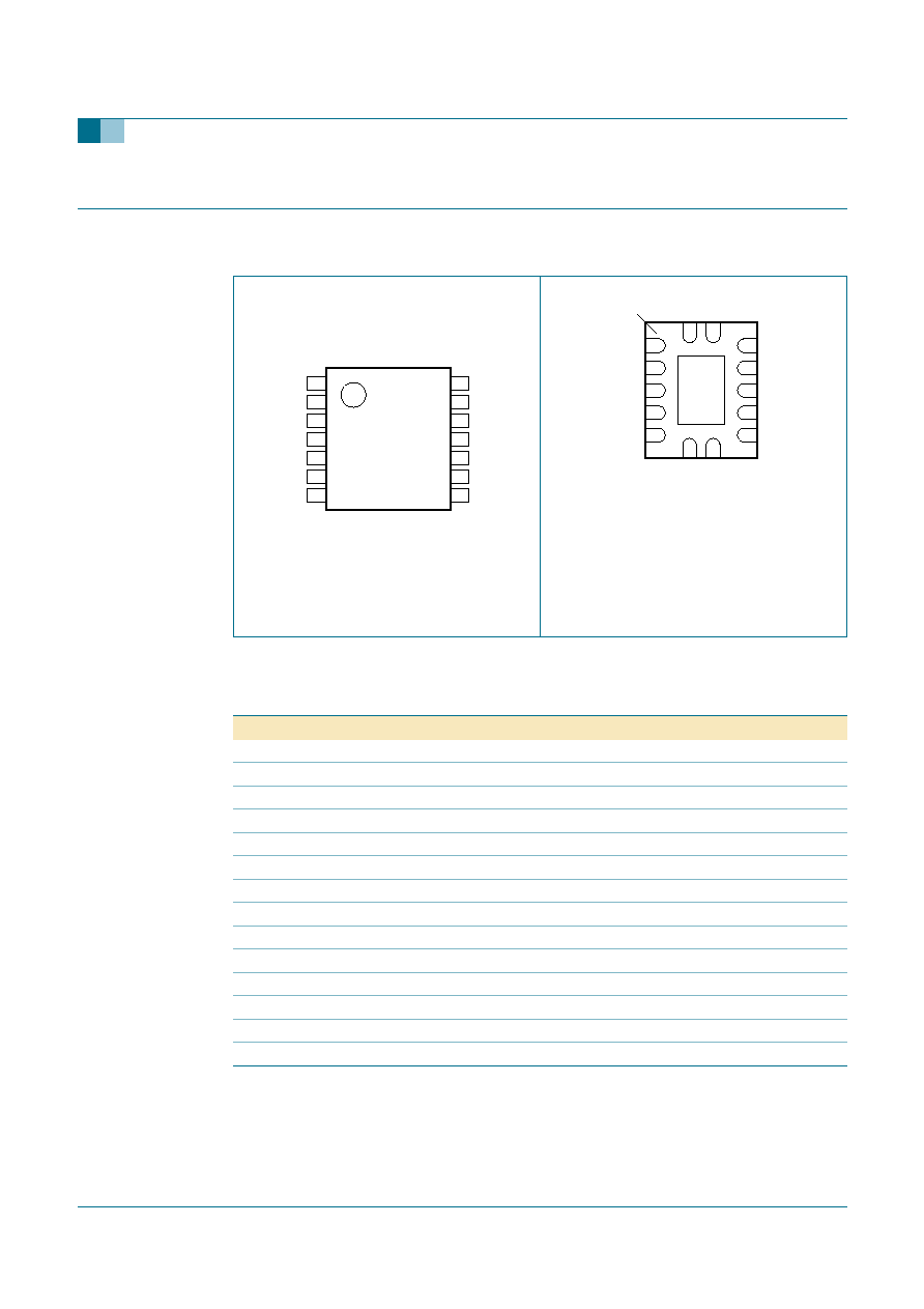
6.1 Pinning
6.2 Pin description
The die substrate is attached to the
exposed die pad using conductive die
attach material. It can not be used as
a supply pin or input.
Fig 4.
Pin configuration SO14 and
TSSOP14
Fig 5.
Pin configuration DHVQFN14
14
1A
V
CC
1Y
6A
2A
6Y
2Y
5A
3A
5Y
3Y
4A
GND
4Y
001aac498
1
2
3
4
5
6
7
8
10
9
12
11
14
13
001aac499
14
GND
(1)
Transparent top view
3Y
4A
3A
5Y
2Y
5A
2A
6Y
1Y
6A
GND
4Y
1A
V
CC
6
9
5
10
4
11
3
12
2
13
7
8
1
14
terminal 1
index area
Table 3:
Pin description
Symbol
Pin
Description
1A
1
1 data input A
1Y
2
1 data output Y
2A
3
2 data input A
2Y
4
2 data output Y
3A
5
3 data input A
3Y
6
3 data output Y
GND
7
ground (0 V)
4Y
8
4 data output Y
4A
9
4 data input A
5Y
10
5 data output Y
5A
11
5 data input A
6Y
12
6 data output Y
6A
13
6 data input A
V
CC
14
supply voltage

9397 750 14592
© Koninklijke Philips Electronics N.V. 2005. All rights reserved.
Product data sheet
Rev. 03 -- 15 February 2005
5 of 16
Philips Semiconductors
74ALVC14
Hex inverting Schmitt trigger
7.
Functional description
7.1 Function table
[1]
H = HIGH voltage level;
L = LOW voltage level.
8.
Limiting values
[1]
The input and output voltage ratings may be exceeded if the input and output current ratings are observed.
[2]
When V
CC
= 0 V (Power-down mode), the output voltage can be 3.6 V in normal operation.
[3]
For SO14 packages: P
tot
derates linearly with 8 mW/K above 70
∞
C.
For TSSOP14 packages: P
tot
derates linearly with 5.5 mW/K above 60
∞
C.
For DHVQFN14 packages: P
tot
derates linearly with 4.5 mW/K above 60
∞
C.
Table 4:
Function table
[1]
Input
Output
nA
nY
L
H
H
L
Table 5:
Limiting values
In accordance with the Absolute Maximum Rating System (IEC 60134). Voltages are referenced to
GND (ground = 0 V).
Symbol Parameter
Conditions
Min
Max
Unit
V
CC
supply voltage
-
0.5
+4.6
V
V
I
input voltage
[1]
-
0.5
+4.6
V
V
O
output voltage
Active mode
[1]
-
0.5
V
CC
+ 0.5 V
Power-down mode
[2]
-
0.5
+4.6
V
I
IK
input diode current
V
I
< 0 V
-
-
50
mA
I
OK
output diode current
V
O
> V
CC
or V
O
< 0 V
-
±
50
mA
I
O
output source or sink
current
V
O
= 0 V to V
CC
-
±
50
mA
I
CC
,
I
GND
V
CC
or GND current
-
±
100
mA
T
stg
storage temperature
-
65
+150
∞
C
P
tot
total power dissipation
T
amb
=
-
40
∞
C to +85
∞
C
[3]
-
500
mW