
Philips Semiconductors
Product data
74ALVCHS16830
18-bit to 36-bit address driver with bus hold (3-State)
2
2002 Mar 15
853-2280 27859
FEATURES
∑
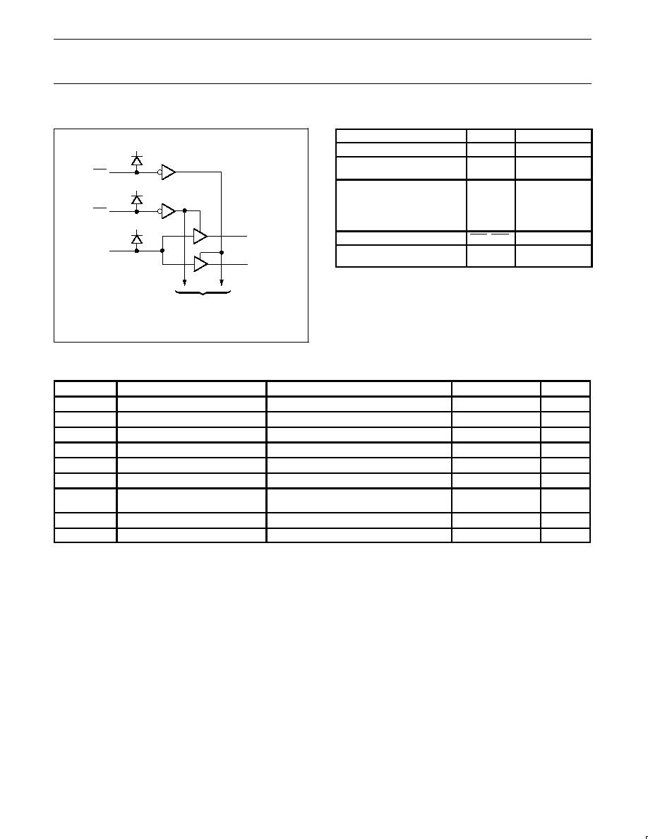
Diodes on inputs clamp overshoot
∑
ESD classification testing is done to JEDEC Standard JESD22.
Protection exceeds 2000 V HBM per method A114.
∑
Latch-up testing is done to JEDEC Standard JESD78, which
exceeds 100 mA.
∑
Bus hold on data inputs eliminates the need for external
pullup/pulldown resistors
∑
Packaged in thin very small-outline package (TVSOP) -- 0.4 mm
pitch
∑
Optimized for use with PCK953 in SDRAM module applications
∑
Low noise, low skew
DESCRIPTION
The ALVCHS16830 address driver is designed for 2.3 V to 3.6 V
V
CC
operation.
Diodes to V
CC
have been added on the inputs to clamp overshoot.
The bus hold feature retains the inputs' last state whenever the input
bus goes to high impedance. This prevents floating inputs and
eliminates the need for pull up or pull down resistors.
To ensure the high-impedance state during power up or power
down, the output-enable (OE) input should be tied to V
CC
through a
pullup resistor; the minimum value of the resistor is determined by
the current-sinking capability of the driver.
The 74ALVCHS16830 is characterized for operation from ≠40 to
+85
∞
C.
FUNCTION TABLE
Inputs
Outputs
OE1
OE2
A
1Yn
2Yn
L
H
H
H
Z
L
H
L
L
Z
H
L
H
Z
H
H
L
L
Z
L
L
L
H
H
H
L
L
L
L
L
H
H
X
Z
Z
PIN CONFIGURATION
1
2
3
4
5
6
7
8
9
10
11
12
69
70
71
72
73
74
75
76
77
78
79
80
2Y2
GND
2Y1
1Y1
V
CC
A1
A2
GND
A3
A4
1Y3
2Y3
GND
1Y4
2Y4
V
CC
1Y5
GND
2Y5
1Y6
2Y6
GND
GND
13
14
15
16
17
18
63
64
65
66
67
68
A5
A6
V
CC
A7
A8
1Y7
V
CC
2Y7
1Y8
2Y8
GND
19
62
GND
A9
20
21
22
23
24
25
56
57
58
59
60
61
OE1
OE2
A10
GND
A11
1Y9
2Y10
2Y9
GND
1Y11
2Y11
A12
26
55 V
CC
V
CC
27
54 1Y12
A13
28
29
30
31
32
49
50
51
52
53
A14
GND
A15
A16
GND
2Y12
1Y13
2Y13
GND
1Y2
GND
1Y10
33
48 1Y14
A17
34
47 2Y14
A18
35
46 V
CC
V
CC
36
37
38
39
40
41
42
43
44
45
2Y18
1Y18
GND
2Y17
1Y17
1Y15
GND
1Y16
2Y16
2Y15
SW00723
TOP VIEW
ORDERING INFORMATION
PACKAGES
TEMPERATURE RANGE
ORDER CODE
DWG NUMBER
80-pin plastic thin very small outline (TVSOP)
≠40 to +85
∞
C
74ALVCHS16830DGB
SOT647-1
Philips Semiconductors
Product data
74ALVCHS16830
18-bit to 36-bit address driver with bus hold (3-State)
2002 Mar 15
3
LOGIC DIAGRAM (POSITIVE LOGIC)
V
CC
SW00724
21
OE2
20
OE1
V
CC
7
A1
V
CC
5
4
1Y1
2Y1
to 17 other channels
PIN DESCRIPTION
PIN(S)
SYMBOL
FUNCTION
6, 15, 26, 35, 46, 55, 66, 75
V
CC
Supply voltage
7, 8, 10, 11, 13, 14, 16, 17, 19,
22, 24, 25, 27, 28, 30, 31, 33, 34
An
Inputs
1, 2, 4, 5, 36, 37, 39, 40, 41, 42,
44, 45, 47, 48, 50, 51, 53, 54,
56, 57, 59, 60, 61, 62, 64, 65,
67, 68, 70, 71, 73, 74, 76, 77,
79, 80
1Yn, 2Yn
Outputs
20, 21
OE1, OE2
Output enable
3, 9, 12, 18, 23, 29, 32, 38, 43,
49, 52, 58, 63, 69, 72, 78
GND
Ground
ABSOLUTE MAXIMUM RATINGS
Over recommended operating free-air temperature range (unless otherwise noted).
1
SYMBOL
PARAMETER
CONDITIONS
RATING
UNIT
V
CC
Supply voltage range
≠0.5 to +4.6
V
V
I
Input voltage range
See Note 2
≠0.5 to +4.6
V
V
O
Output voltage range
See Notes 2 and 3
≠0.5 to V
CC
+0.5
V
I
IK
Input clamp current
V
I
< 0
≠50
mA
I
OK
Output clamp current
V
O
< 0
≠50
mA
I
O
Continuous output current
"
50
mA
I
CC
, I
GND
Continuous current through each V
CC
or GND
"
100
mA
JA
Package thermal impedance
See Note 4
106
∞
C/W
T
stg
Storage temperature range
≠65 to +150
∞
C
NOTES:
1. Stresses beyond those listed under "absolute maximum ratings" may cause permanent damage to the device. These are stress ratings
only, and functional operation of the device at these or any other conditions beyond those indicated under "recommended operating
conditions" is not implied. Exposure to absolute-maximum-rated conditions for extended periods may affect device reliability.
2. The input negative-voltage and output voltage ratings may be exceeded if the input and output current ratings are observed.
3. This value is limited to 4.6 V maximum.
4. The package thermal impedance is calculated in accordance with JESD 51.


