1.
General description
The 74AUP1G125 is a high-performance, low-power, low-voltage, Si-gate CMOS device,
superior to most advanced CMOS compatible TTL families.
Schmitt-trigger action at all inputs makes the circuit tolerant to slower input rise and fall
times across the entire V
CC
range from 0.8 V to 3.6 V.
This device ensures a very low static and dynamic power consumption across the entire
V
CC
range from 0.8 V to 3.6 V.
This device is fully specified for partial Power-down applications using I
OFF
.
The I
OFF
circuitry disables the output, preventing the damaging backflow current through
the device when it is powered down.
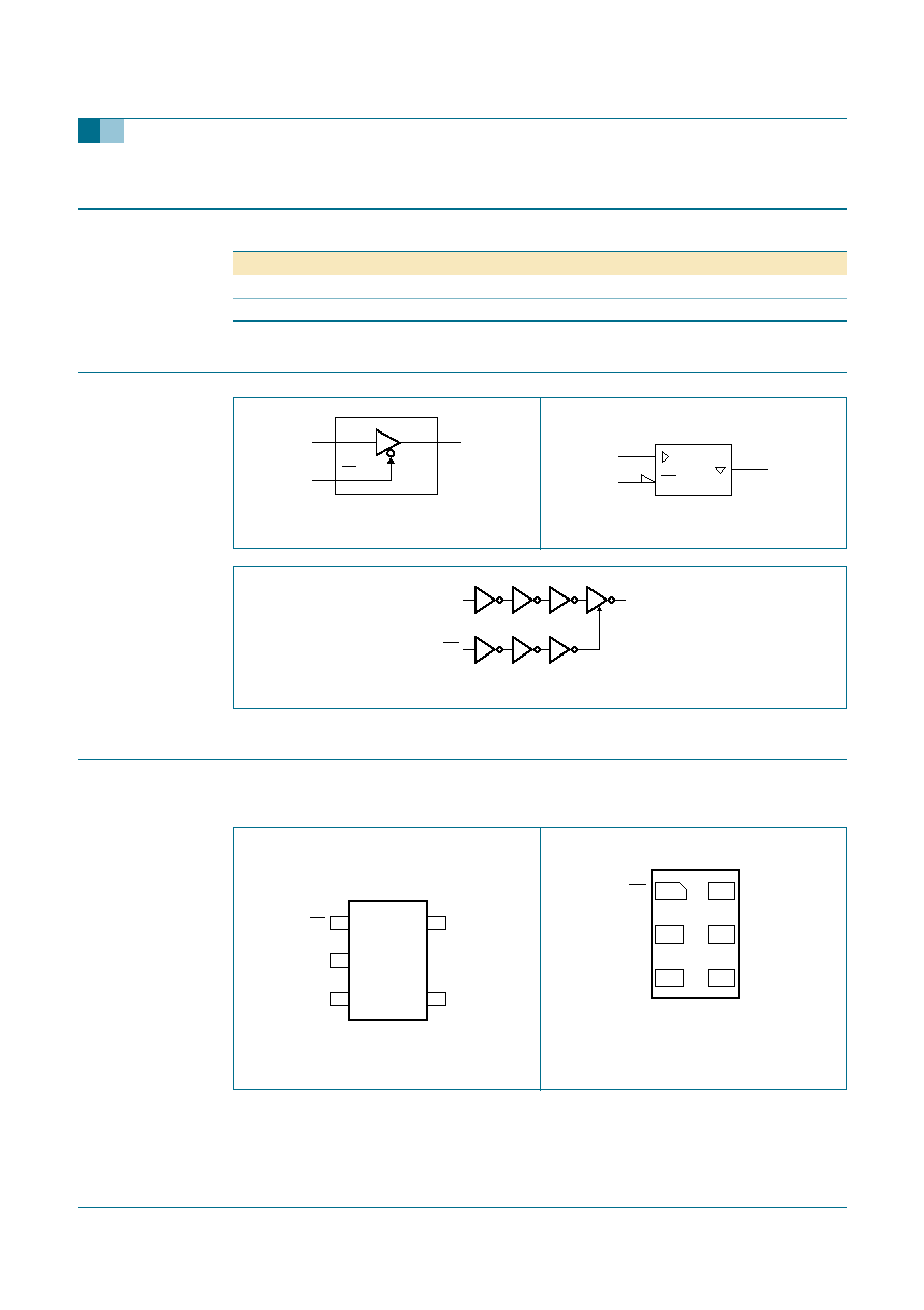
The 74AUP1G125 provides the single non-inverting buffer/line driver with 3-state output.
The 3-state output is controlled by the output enable input (OE). A HIGH level at pin OE
causes the output to assume a high-impedance OFF-state.
This device has the input-disable feature, which allows floating input signals. The inputs
are disabled when the output enable input OE) is HIGH.
2.
Features
s
Wide supply voltage range from 0.8 V to 3.6 V
s
High noise immunity
s
Complies with JEDEC standards:
x
JESD8-12 (0.8 V to 1.3 V)
x
JESD8-11 (0.9 V to 1.65 V)
x
JESD8-7 (1.2 V to 1.95 V)
x
JESD8-5 (1.8 V to 2.7 V)
x
JESD8-B (2.7 V to 3.6 V)
s
ESD protection:
x
HBM JESD22-A114-C exceeds 2000 V
x
MM JESD22-A115-A exceeds 200 V
x
CDM JESD22-C101-C exceeds 1000 V
s
Low static power consumption; I
CC
= 0.9
µ
A (maximum)
s
Latch-up performance exceeds 100 mA per JESD 78 Class II
s
Inputs accept voltages up to 3.6 V
s
Low noise overshoot and undershoot < 10 % of V
CC
s
Input-disable feature allows floating input conditions
74AUP1G125
Low-power buffer/line driver; 3-state
Rev. 01 -- 18 July 2005
Product data sheet

9397 750 14685
© Koninklijke Philips Electronics N.V. 2005. All rights reserved.
Product data sheet
Rev. 01 -- 18 July 2005
2 of 20
Philips Semiconductors
74AUP1G125
Low-power buffer/line driver; 3-state
s
I
OFF
circuitry provides partial Power-down mode operation
s
Multiple package options
s
Specified from
-
40
∞
C to +85
∞
C and
-
40
∞
C to +125
∞
C
3.
Quick reference data
[1]
C
PD
is used to determine the dynamic power dissipation (P
D
in
µ
W).
P
D
= C
PD
◊
V
CC
2
◊
f
i
◊
N +
(C
L
◊
V
CC
2
◊
f
o
) where:
f
i
= input frequency in MHz;
f
o
= output frequency in MHz;
C
L
= output load capacitance in pF;
V
CC
= supply voltage in V;
N = number of inputs switching;
(C
L
◊
V
CC
2
◊
f
o
) = sum of the outputs.
[2]
The condition is V
I
= GND to V
CC
.
4.
Ordering information
Table 1:
Quick reference data
GND = 0 V; T
amb
= 25
∞
C; t
r
= t
f
3 ns.
Symbol
Parameter
Conditions
Min
Typ
Max Unit
t
PHL
, t
PLH
propagation delay
A to Y
C
L
= 5 pF; R
L
= 1 M
;
V
CC
= 0.8 V
-
20.6
-
ns
C
L
= 5 pF; R
L
= 1 M
;
V
CC
= 1.1 V to 1.3 V
2.8
5.5
11.8 ns
C
L
= 5 pF; R
L
= 1 M
;
V
CC
= 1.4 V to 1.6 V
2.2
3.9
7.0
ns
C
L
= 5 pF; R
L
= 1 M
;
V
CC
= 1.65 V to 1.95 V
1.9
3.2
5.5
ns
C
L
= 5 pF; R
L
= 1 M
;
V
CC
= 2.3 V to 2.7 V
1.7
2.6
4.1
ns
C
L
= 5 pF; R
L
= 1 M
;
V
CC
= 3.0 V to 3.6 V
1.7
2.4
3.7
ns
C
i
input capacitance
-
0.9
-
pF
C
PD
power dissipation
capacitance
f = 10 MHz; output enabled
[1] [2]
V
CC
= 1.8 V
-
3.5
-
pF
V
CC
= 3.3 V
-
4.4
-
pF
f = 10 MHz; output disabled
[1] [2]
V
CC
= 0.8 V to 3.6 V
-
0
-
pF
Table 2:
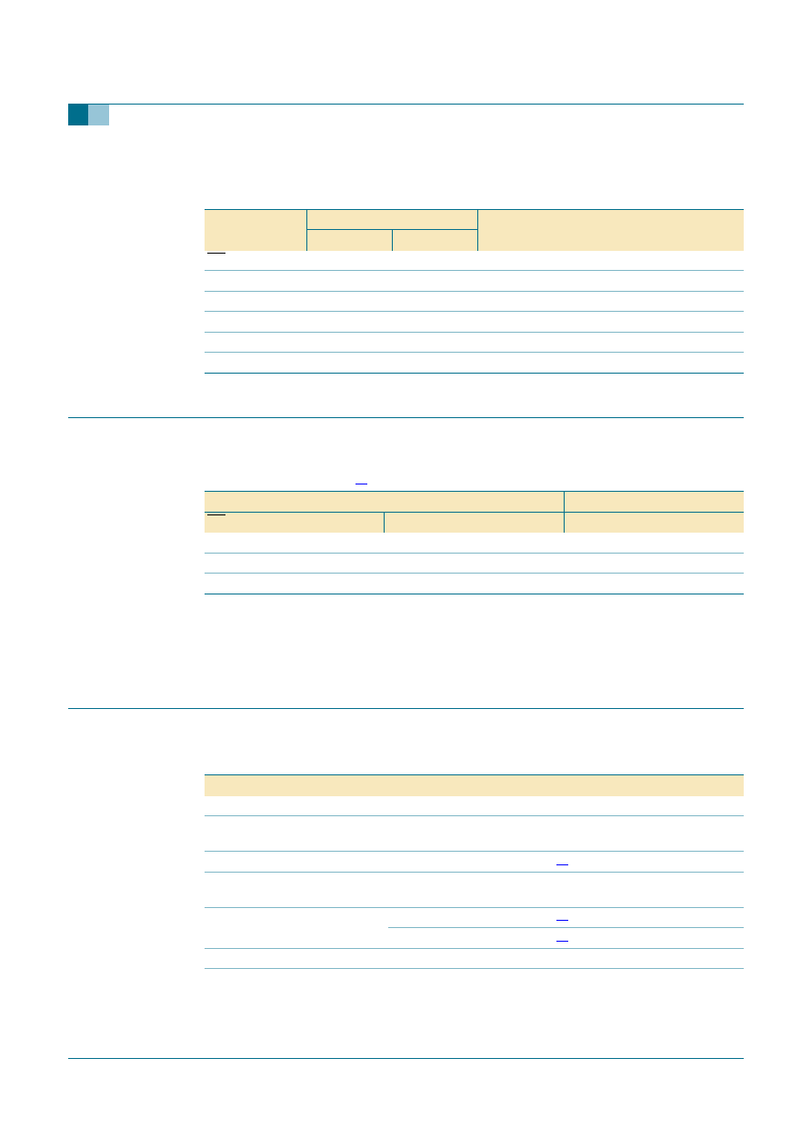
Ordering information
Type number
Package
Temperature range
Name
Description
Version
74AUP1G125GW
-
40
∞
C to +125
∞
C
TSSOP5
plastic thin shrink small outline package; 5 leads;
body width 1.25 mm
SOT353-1
74AUP1G125GM
-
40
∞
C to +125
∞
C
XSON6
plastic extremely thin small outline package; no leads;
6 terminals; body 1
◊
1.45
◊
0.5 mm
SOT886
9397 750 14685
© Koninklijke Philips Electronics N.V. 2005. All rights reserved.
Product data sheet
Rev. 01 -- 18 July 2005
4 of 20
Philips Semiconductors
74AUP1G125
Low-power buffer/line driver; 3-state
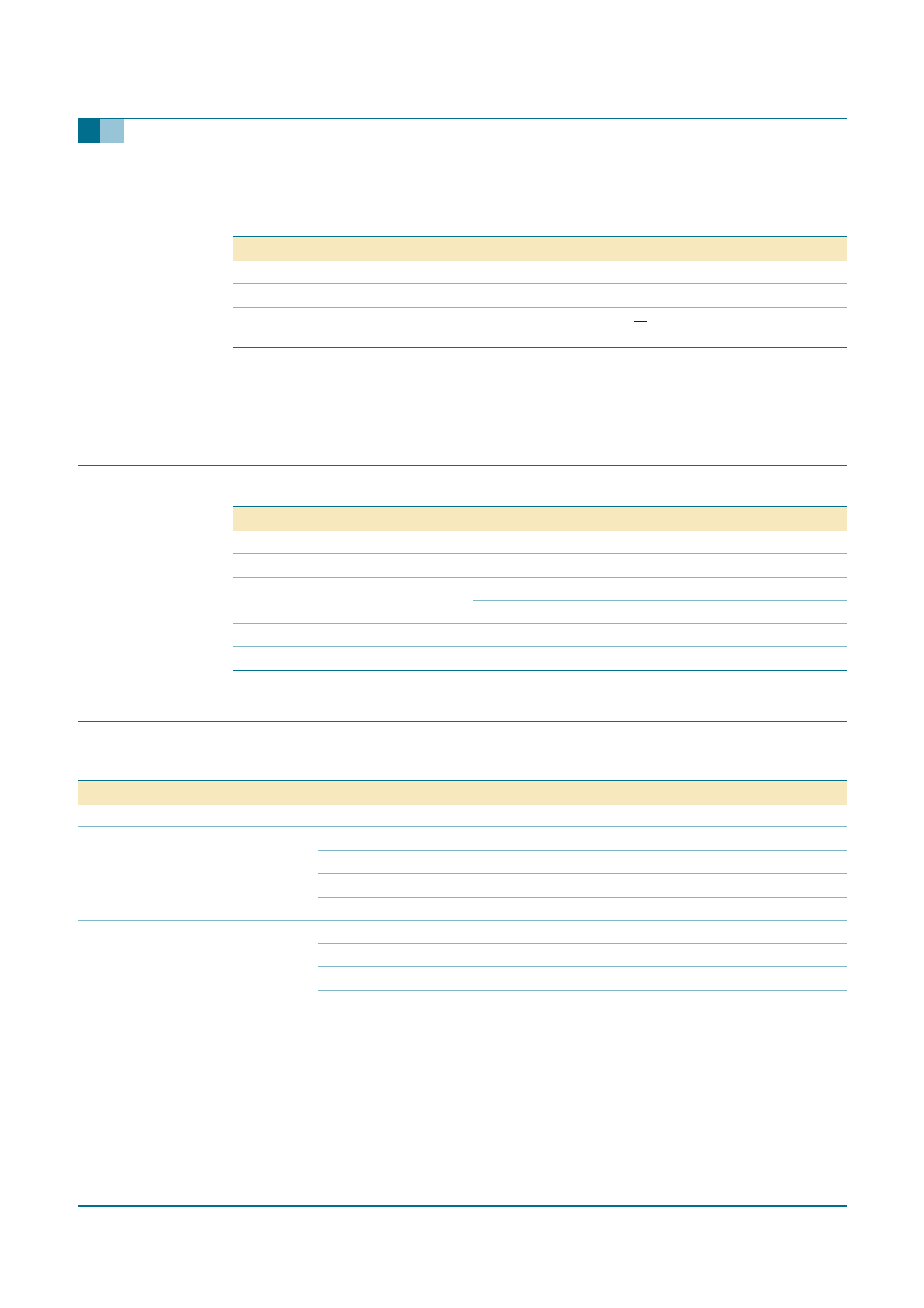
7.2 Pin description
8.
Functional description
8.1 Function table
[1]
H = HIGH voltage level;
L = LOW voltage level;
X = Don't care;
Z = high-impedance OFF-state.
9.
Limiting values
Table 4:
Pin description
Symbol
Pin
Description
TSSOP5
XSON6
OE
1
1
output enable input
A
2
2
data input A
GND
3
3
ground (0 V)
Y
4
4
data output Y
n.c.
-
5
not connected
V
CC
5
6
supply voltage
Table 5:
Function table
[1]
Input
Output
OE
A
Y
L
L
L
L
H
H
H
X
Z
Table 6:
Limiting values
In accordance with the Absolute Maximum Rating System (IEC 60134). Voltages are referenced to
GND (ground = 0 V).
Symbol
Parameter
Conditions
Min
Max
Unit
V
CC
supply voltage
-
0.5
+4.6
V
I
IK
input clamping
current
V
I
< 0 V
-
-
50
mA
V
I
input voltage
[1]
-
0.5
+4.6
V
I
OK
output clamping
current
V
O
> V
CC
or V
O
< 0 V
-
±
50
mA
V
O
output voltage
active mode
[1]
-
0.5
V
CC
+ 0.5 V
Power-down mode
[1]
-
0.5
+4.6
V
I
O
output current
V
O
= 0 V to V
CC
-
±
20
mA
I
CC
quiescent supply
current
-
+50
mA
9397 750 14685
© Koninklijke Philips Electronics N.V. 2005. All rights reserved.
Product data sheet
Rev. 01 -- 18 July 2005
5 of 20
Philips Semiconductors
74AUP1G125
Low-power buffer/line driver; 3-state
[1]
The input and output voltage ratings may be exceeded if the input and output current ratings are observed.
[2]
For TSSOP5 packages: above 87.5
∞
C the value of P
tot
derates linearly with 4.0 mW/K.
For XSON6 packages: above 45
∞
C the value of P
tot
derates linearly with 2.4 mW/K.
10. Recommended operating conditions
11. Static characteristics
I
GND
ground current
-
-
50
mA
T
stg
storage temperature
-
65
+150
∞
C
P
tot
total power
dissipation
T
amb
=
-
40
∞
C to +125
∞
C
[2]
-
250
mW
Table 6:
Limiting values
...continued
In accordance with the Absolute Maximum Rating System (IEC 60134). Voltages are referenced to
GND (ground = 0 V).
Symbol
Parameter
Conditions
Min
Max
Unit
Table 7:
Recommended operating conditions
Symbol
Parameter
Conditions
Min
Max
Unit
V
CC
supply voltage
0.8
3.6
V
V
I
input voltage
0
3.6
V
V
O
output voltage
active mode
0
V
CC
V
Power-down mode; V
CC
= 0 V
0
3.6
V
T
amb
ambient temperature
-
40
+125
∞
C
t
r
, t
f
input rise and fall times
V
CC
= 0.8 V to 3.6 V
0
200
ns/V
Table 8:
Static characteristics
At recommended operating conditions; voltages are referenced to GND (ground = 0 V).
Symbol Parameter
Conditions
Min
Typ
Max
Unit
T
amb
= 25
∞
C
V
IH
HIGH-state input voltage
V
CC
= 0.8 V
0.70
◊
V
CC
-
-
V
V
CC
= 0.9 V to 1.95 V
0.65
◊
V
CC
-
-
V
V
CC
= 2.3 V to 2.7 V
1.6
-
-
V
V
CC
= 3.0 V to 3.6 V
2.0
-
-
V
V
IL
LOW-state input voltage
V
CC
= 0.8 V
-
-
0.30
◊
V
CC
V
V
CC
= 0.9 V to 1.95 V
-
-
0.35
◊
V
CC
V
V
CC
= 2.3 V to 2.7 V
-
-
0.7
V
V
CC
= 3.0 V to 3.6 V
-
-
0.9
V