Document Outline
- FEATURES
- DESCRIPTION
- PIN CONFIGURATION
- QUICK REFERENCE DATA
- ORDERING INFORMATION
- PIN DESCRIPTION
- LOGIC SYMBOL
- LOGIC SYMBOL (IEEE/IEC)
- FUNCTION TABLE
- RECOMMENDED OPERATING CONDITIONS
- ABSOLUTE MAXIMUM RATINGS
- DC ELECTRICAL CHARACTERISTICS
- AC CHARACTERISTICS
- AC WAVEFORMS
- TEST CIRCUIT
- GRAPHS
- PACKAGE
- Data sheet status
- Definitions
- Disclaimers
Philips
Semiconductors
74AVC16334A
16-bit registered driver with
inverted register enable and
Dynamic Controlled Outputs
TM
(3-State)
Product specification
Supersedes data of 2000 May 02
2000 Aug 03
INTEGRATED CIRCUITS

Philips Semiconductors
Product specification
74AVC16334A
16-bit registered driver with inverted register enable and
Dynamic Controlled Outputs
TM
(3-State)
2
2000 Aug 03
853-2212 24282
FEATURES
∑
Wide supply voltage range of 1.2 V to 3.6 V
∑
Complies with JEDEC standard no. 8-1A/5/7.
∑
CMOS low power consumption
∑
Input/output tolerant up to 3.6 V
∑
DCO (Dynamic Controlled Output) circuit dynamically changes
output impedance, resulting in noise reduction without speed
degradation
∑
Low inductance multiple V
CC
and GND pins for minimum noise
and ground bounce
∑
Power off disables 74AVC16334A outputs, permitting Live
Insertion
∑
Integrated input diodes to minimize input overshoot and
undershoot
∑
Full PC133 solution provided when used with PCK2509S or
PCK2510S and CBT16292
DESCRIPTION
The 74AVC16334A is a 16-bit universal bus driver. Data flow is
controlled by output enable (OE), latch enable (LE) and clock inputs
(CP).
This product is designed to have an extremely fast propagation
delay and a minimum amount of power consumption.
To ensure the high-impedance state during power up or power
down, OE should be tied to V
CC
through a pullup resistor (Live
Insertion).
A Dynamic Controlled Output (DCO) circuitry is implemented to
support termination line drive during transient. See the graphs on
page 8 for typical curves.
PIN CONFIGURATION
1
2
3
4
5
6
7
8
9
10
11
12
13
14
15
16
17
18
19
20
21
22
23
24
28
27
26
25
29
30
31
32
33
34
35
36
37
38
39
40
41
42
43
44
45
46
47
48
OE
Y
0
Y
1
Y
2
Y
3
Y
4
Y
5
GND
GND
V
CC
Y
6
Y
7
Y
8
Y
9
GND
Y
10
Y
11
V
CC
Y
12
Y
13
GND
Y
14
Y
15
NC
CP
A
0
A
1
GND
A
2
A
3
V
CC
A
4
A
5
GND
A
6
A
7
A
8
A
9
GND
A
10
A
11
V
CC
A
12
A
13
GND
A
14
A
15
LE
SH00167
QUICK REFERENCE DATA
GND = 0 V; T
amb
= 25
∞
C; t
r
= t
f
2.0 ns; C
L
= 30 pF.
SYMBOL
PARAMETER
CONDITIONS
TYPICAL
UNIT
t
PHL
/t
PLH
Propagation delay
An to Yn
V
CC
= 1.8 V
V
CC
= 2.5 V
V
CC
= 3.3 V
2.5
1.7
1.5
ns
t
PHL
/t
PLH
Propagation delay
LE to Yn;
CP to Yn
V
CC
= 1.8 V
V
CC
= 2.5 V
V
CC
= 3.3 V
2.7
2.0
1.6
ns
C
I
Input capacitance
3.8
pF
C
Power dissipation capacitance per buffer
V = GND to V
CC
1
Outputs enabled
25
pF
C
PD
Power dissipation capacitance per buffer
V
I
= GND to V
CC
1
Output disabled
6
pF
NOTE:
1. C
PD
is used to determine the dynamic power dissipation (P
D
in
µ
W):
P
D
= C
PD
◊
V
CC
2
◊
f
i
+
S
(C
L
◊
V
CC
2
◊
f
o
) where: f
i
= input frequency in MHz; C
L
= output load capacitance in pF;
f
o
= output frequency in MHz; V
CC
= supply voltage in V;
S
(C
L
◊
V
CC
2
◊
f
o
) = sum of outputs.
ORDERING INFORMATION
PACKAGES
TEMPERATURE
RANGE
OUTSIDE NORTH
AMERICA
NORTH AMERICA
DRAWING
NUMBER
48-Pin Plastic Thin Shrink Small Outline (TSSOP) Type II
≠40
∞
C to +85
∞
C
AVC16334A DGG
SOT362-1
Philips Semiconductors
Product specification
74AVC16334A
16-bit registered driver with inverted register enable and
Dynamic Controlled Outputs
TM
(3-State)
2000 Aug 03
3
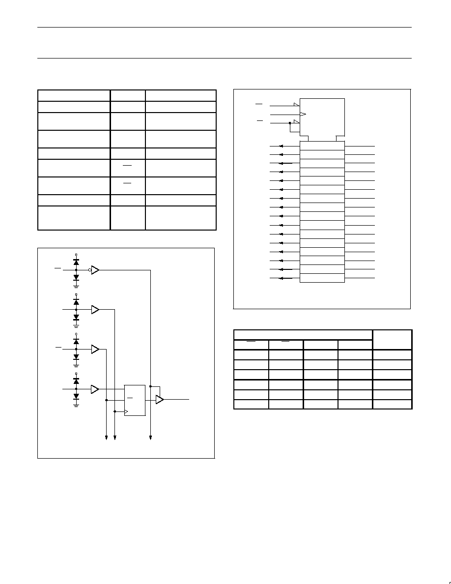
PIN DESCRIPTION
PIN NUMBER
SYMBOL
NAME AND FUNCTION
24
NC
No connection
2, 3, 5, 6, 8, 9, 11, 12, 13,
14, 16, 17, 19, 20, 22, 23
Y
0
to Y
15
Data outputs
4, 10, 15, 21, 28, 34, 39,
45
GND
Ground (0 V)
7, 18, 31, 42
V
CC
Positive supply voltage
1
OE
Output enable input
(active LOW)
25
LE
Latch enable input
(active LOW)
48
CLK
Clock input
47, 46, 44, 43, 41, 40,
38, 37, 36, 35, 33, 32,
30, 29, 27, 26
A
0
to A
15
Data inputs
LOGIC SYMBOL
SH00202
CP
LE
D
OE
LE
A
1
Y
1
TO THE 17 OTHER CHANNELS
CP
LOGIC SYMBOL (IEEE/IEC)
11
1
48
25
47
46
44
43
41
40
38
37
36
35
33
32
30
29
27
26
2
3
5
6
8
9
11
12
13
14
16
17
19
20
22
23
3D
1
2C3
EN1
A
0
A
1
A
2
A
3
A
4
A
5
A
6
A
7
A
8
A
9
A
10
A
11
A
12
A
13
A
14
A
15
OE
CP
Y
0
Y
1
Y
2
Y
3
Y
4
Y
5
Y
6
Y
7
Y
8
Y
9
Y
10
Y
11
Y
12
Y
13
Y
14
Y
15
LE
C3
G2
SH00168
FUNCTION TABLE
INPUTS
OUTPUTS
OE
LE
CLK
A
OUTPUTS
H
X
X
X
Z
L
L
X
L
L
L
L
X
H
H
L
H
L
L
L
H
H
H
L
H
L or H
X
Y
0
1
H
=
HIGH voltage level
L
=
LOW voltage level
X
=
Don't care
Z
=
High impedance "off" state
=
LOW-to-HIGH level transition
NOTE:
1. Output level before the indicated steady-state input conditions
were established.
Philips Semiconductors
Product specification
74AVC16334A
16-bit registered driver with inverted register enable and
Dynamic Controlled Outputs
TM
(3-State)
2000 Aug 03
4
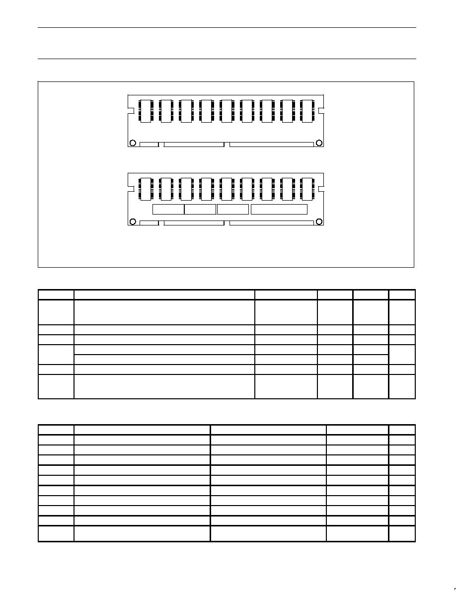
168-pin SDR SDRAM DIMM
SDRAM
SDRAM
SDRAM
SDRAM
SDRAM
SDRAM
SDRAM
SDRAM
SDRAM
The PLL clock distribution device and AVC registered drivers reduce
signal loads on the memory controller and prevent timing delays and
waveform distortions that would cause unreliable operation
SDRAM
SDRAM
SDRAM
SDRAM
SDRAM
SDRAM
SDRAM
SDRAM
SDRAM
74AVC16334A
PCK2509S or PCK2510S
74AVC16334A
BACK SIDE
FRONT SIDE
74AVC16334A
SW00525
RECOMMENDED OPERATING CONDITIONS
SYMBOL
PARAMETER
CONDITIONS
MIN
MAX
UNIT
DC supply voltage
1.65
1.95
V
CC
DC supply voltage
(according to JEDEC Low Voltage Standards)
2.3
2.7
V
(according to JEDEC Low Voltage Standards)
3.0
3.6
V
CC
DC supply voltage (for low voltage applications)
1.2
3.6
V
V
I
DC Input voltage range
0
3.6
V
V
O
DC output voltage range; output 3-State
0
3.6
V
V
O
DC output voltage range; output HIGH or LOW state
0
V
CC
V
T
amb
Operating free-air temperature range
≠40
+85
∞
C
V
CC
= 1.65 to 2.3 V
0
30
t
r
, t
f
Input rise and fall times
V
CC
= 2.3 to 3.0 V
0
20
ns/V
V
CC
= 3.0 to 3.6 V
0
10
ABSOLUTE MAXIMUM RATINGS
In accordance with the Absolute Maximum Rating System (IEC 134). Voltages are referenced to GND (ground = 0 V).
SYMBOL
PARAMETER
CONDITIONS
RATING
UNIT
V
CC
DC supply voltage
≠0.5 to +4.6
V
I
IK
DC input diode current
V
I
t
0
≠50
mA
V
I
DC input voltage
For data inputs
1
≠0.5 to 4.6
V
I
OK
DC output diode current
V
O
u
V
CC
or V
O
t
0
"
50
mA
V
O
DC output voltage; output 3-State
Note 1
≠0.5 to 4.6
V
V
O
DC output voltage; output HIGH or LOW state
Note 1
≠0.5 to V
CC
+0.5
V
I
O
DC output source or sink current
V
O
= 0 to V
CC
"
50
mA
I
GND
, I
CC
DC V
CC
or GND current
"
100
mA
T
stg
Storage temperature range
≠65 to +150
∞
C
P
TOT
Power dissipation per package
≠plastic thin-medium-shrink (TSSOP)
For temperature range: ≠40 to +125
∞
C
above +55
∞
C derate linearly with 8 mW/K
600
mW
NOTE:
1. The input and output voltage ratings may be exceeded if the input and output current ratings are observed.
Philips Semiconductors
Product specification
74AVC16334A
16-bit registered driver with inverted register enable and
Dynamic Controlled Outputs
TM
(3-State)
2000 Aug 03
5
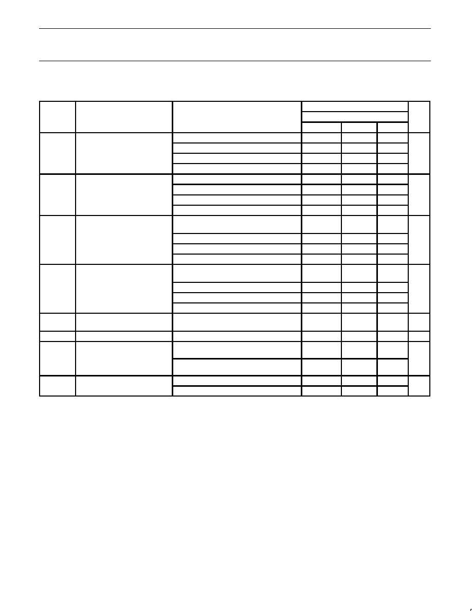
DC ELECTRICAL CHARACTERISTICS
Over recommended operating conditions. Voltage are referenced to GND (ground = 0 V).
LIMITS
SYMBOL
PARAMETER
TEST CONDITIONS
Temp = -40
∞
C to +85
∞
C
UNIT
MIN
TYP
1
MAX
V
CC
= 1.2 V
V
CC
≠
≠
V
HIGH level Input voltage
V
CC
= 1.65 to 1.95 V
0.65 V
CC
0.9
≠
V
V
IH
HIGH level Input voltage
V
CC
= 2.3 to 2.7 V
1.7
1.2
≠
V
V
CC
= 3.0 to 3.6 V
2.0
1.5
≠
V
CC
= 1.2 V
≠
≠
GND
V
LOW level Input voltage
V
CC
= 1.65 to 1.95 V
≠
0.9
0.35 V
CC
V
V
IL
LOW level Input voltage
V
CC
= 2.3 to 2.7 V
≠
1.2
0.7
V
V
CC
= 3.0 to 3.6 V
≠
1.5
0.8
V
CC
= 1.65 to 3.6 V; V
I
= V
IH
or V
IL
;
V
CC
0 20
V
CC
CC
I
IH
IL
I
O
= ≠100
µ
A
V
CC
*
0.20
V
CC
≠
V
OH
HIGH level output voltage
V
CC
= 1.65 V; V
I
= V
IH
or V
IL
; I
O
= ≠4 mA
V
CC
*
0.45
V
CC
*
0.10
≠
V
OH
g
V
CC
= 2.3 V; V
I
= V
IH
or V
IL
; I
O
= ≠8 mA
V
CC
*
0.55
V
CC
*
0.28
≠
V
CC
= 3.0 V; V
I
= V
IH
or V
IL
; I
O
= ≠12 mA
V
CC
*
0.70
V
CC
*
0.32
≠
V
CC
= 1.65 to 3.6 V; V
I
= V
IH
or V
IL
;
GND
0 20
CC
I
IH
IL
I
O
= 100
µ
A
≠
GND
0.20
V
OL
LOW level output voltage
V
CC
= 1.65 V; V
I
= V
IH
or V
IL
; I
O
= 4 mA
≠
0.10
0.45
V
OL
g
V
CC
= 2.3 V; V
I
= V
IH
or V
IL
; I
O
= 8 mA
≠
0.26
0.55
V
CC
= 3.0 V; V
I
= V
IH
or V
IL
; I
O
= 12 mA
≠
0.36
0.70
V
CC
= 3 6 V;
I
I
Input leakage current
V
CC
= 3.6 V;
V
V
or GND
≠
0.1
2.5
µ
A
I
I
In ut leakage current
V
I
= V
CC
or GND
0.1
2.5
µ
A
I
OFF
3-State output OFF-state current
V
CC
= 0 V; V
I
or V
O
= 3.6 V
≠
0.1
"
10
µ
A
I
O
3 State output OFF state current
V
CC
= 1.65 to 2.7 V; V
I
= V
IH
or V
IL
;
V
O
= V
CC
or GND
≠
0.1
5
µ
A
I
OZ
3-State output OFF-state current
V
CC
= 3.0 to 3.6 V; V
I
= V
IH
or V
IL
;
V
O
= V
CC
or GND
≠
0.1
10
µ
A
I
CC
Quiescent supply current
V
CC
= 1.65 to 2.7 V; V
I
= V
CC
or GND; I
O
= 0
≠
0.1
20
µ
A
I
CC
Quiescent supply current
V
CC
= 3.0 to 3.6 V; V
I
= V
CC
or GND; I
O
= 0
≠
0.2
40
µ
A
NOTE:
1. All typical values are at T
amb
= 25
∞
C.