Philips
Semiconductors
74AVC16835
18-bit registered driver (3-State)
Preliminary specification
Replaces datasheet 74AVC16835/74AVCH16835 dated 1998 Dec 07
1999 Jul 23
INTEGRATED CIRCUITS

Philips Semiconductors
Preliminary specification
74AVC16835
18-bit Registered Driver (3-State)
2
1999 Jul 23
FEATURES
∑
Wide supply voltage range of 1.2 V to 3.6 V
∑
Complies with JEDEC standard no. 8-1A/5/7.
∑
CMOS low power consumption
∑
Input/output tolerant up to 3.6 V
∑
DCO (Dynamic Controlled Output) circuit dynamically changes
output impedance, resulting in noise reduction without speed
degradation
∑
Low inductance multiple V
CC
and GND pins for minimum noise
and ground bounce
∑
Power off disables 74AVC16835 outputs, permitting Live Insertion
DESCRIPTION
The 74AVC16835 is a 18-bit universal bus driver. Data flow is
controlled by output enable (OE), latch enable (LE) and clock inputs
(CP).
This product is designed to have an extremely fast propagation
delay and a minimum amount of power consumption.
To ensure the high-impedance state during power up or power
down, OE should be tied to V
CC
through a pullup resistor (Live
Insertion).
A Dynamic Controlled Output (DCO) circuitry is implemented to
support termination line drive during transient. See the graphs on
page 8 for typical curves.
PIN CONFIGURATION
1
2
3
4
5
6
7
8
9
10
11
12
13
14
15
16
17
18
19
20
21
22
23
24
25
26
27
28
29
30
31
32
33
34
35
36
37
38
39
40
41
42
43
44
45
46
47
48
49
50
51
52
53
54
55
56
NC
NC
Y
0
Y
1
Y
2
Y
3
Y
4
Y
5
GND
V
CC
GND
Y
6
Y
7
Y
8
Y
9
Y
10
Y
11
GND
Y
12
Y
13
Y
14
V
CC
Y
15
Y
16
GND
Y
17
OE
LE
GND
NC
A
0
GND
A
1
A
2
V
CC
A
3
A
4
A
5
GND
A
6
A
7
A
8
A
9
A
10
A
11
GND
A
12
A
13
A
14
V
CC
A
15
A
16
GND
A
17
CP
GND
SH00130
QUICK REFERENCE DATA
GND = 0 V; T
amb
= 25
∞
C; t
r
= t
f
2.0 ns; C
L
= 30 pF.
SYMBOL
PARAMETER
CONDITIONS
TYPICAL
UNIT
t
PHL
/t
PLH
Propagation delay
An to Yn
V
CC
= 1.8 V
V
CC
= 2.5 V
V
CC
= 3.3 V
2.6
2.0
1.7
ns
t
PHL
/t
PLH
Propagation delay
LE to Yn;
CP to Yn
V
CC
= 1.8 V
V
CC
= 2.5 V
V
CC
= 3.3 V
2.8
2.2
1.8
ns
C
I
Input capacitance
5.0
pF
C
PD
Power dissipation capacitance per buffer
V
I
= GND to V
CC
1
Outputs enabled
25
pF
C
PD
Power dissi ation ca acitance er buffer
V
I
= GND to V
CC
1
Output disabled
6
F
NOTES:
1. C
PD
is used to determine the dynamic power dissipation (P
D
in
µ
W):
P
D
= C
PD
◊
V
CC
2
◊
f
i
+
S
(C
L
◊
V
CC
2
◊
f
o
) where: f
i
= input frequency in MHz; C
L
= output load capacitance in pF;
f
o
= output frequency in MHz; V
CC
= supply voltage in V;
S
(C
L
◊
V
CC
2
◊
f
o
) = sum of outputs.
ORDERING INFORMATION
PACKAGES
TEMPERATURE
RANGE
ORDER CODE
DRAWING
NUMBER
56-Pin Plastic Thin Shrink Small Outline (TSSOP) Type II
≠40
∞
C to +85
∞
C
74AVC16835 DGG
SOT364-1
Philips Semiconductors
Preliminary specification
74AVC16835
18-bit Registered Driver (3-State)
1999 Jul 23
3
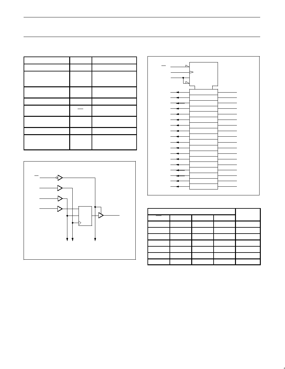
PIN DESCRIPTION
PIN NUMBER
SYMBOL
NAME AND FUNCTION
1, 2, 55
NC
No connection
3, 5, 6, 8, 9, 10, 12, 13,
14, 15, 16, 17, 19, 20,
21, 23, 24, 26
Y
0
to Y
17
Data outputs
4, 11, 18, 25, 32, 39, 46,
53, 56
GND
Ground (0V)
7, 22, 35, 50
V
CC
Positive supply voltage
27
OE
Output enable input
(active LOW)
28
LE
Latch enable input
(active HIGH)
30
CP
Clock input
54, 52, 51, 49, 48, 47,
45, 44, 43, 42, 41, 40,
38, 37, 36, 34, 33, 31
A
0
to A
17
Data inputs
LOGIC SYMBOL
SH00138
CP
LE
D
OE
CP
LE
A
0
Y
0
TO THE 17 OTHER CHANNELS
LOGIC SYMBOL (IEEE/IEC)
1
1
30
28
54
52
51
49
48
47
45
44
43
42
41
40
38
37
36
34
33
31
3
5
6
8
9
10
12
13
14
15
16
17
19
20
21
23
24
26
3D
27
2C3
EN1
A
0
A
1
A
2
A
3
A
4
A
5
A
6
A
7
A
8
A
9
A
10
A
11
A
12
A
13
A
14
A
15
A
16
A
17
OE
CP
Y
0
Y
1
Y
2
Y
3
Y
4
Y
5
Y
6
Y
7
Y
8
Y
9
Y
10
Y
11
Y
12
Y
13
Y
14
Y
15
Y
16
Y
17
LE
C3
G2
SH00154
FUNCTION TABLE
INPUTS
OUTPUTS
OE
LE
CP
A
OUTPUTS
H
X
X
X
Z
L
H
X
L
L
L
H
X
H
H
L
L
L
L
L
L
H
H
L
L
H
X
Y
0
1
L
L
L
X
Y
0
2
H
=
HIGH voltage level
L
=
LOW voltage level
X
=
Don't care
Z
=
High impedance "off" state
=
LOW-to-HIGH level transition
NOTES:
1. Output level before the indicated steady-state input conditions
were established, provided that CP is high before LE goes low.
2. Output level before the indicated steady-state input conditions
were established.
Philips Semiconductors
Preliminary specification
74AVC16835
18-bit Registered Driver (3-State)
1999 Jul 23
4
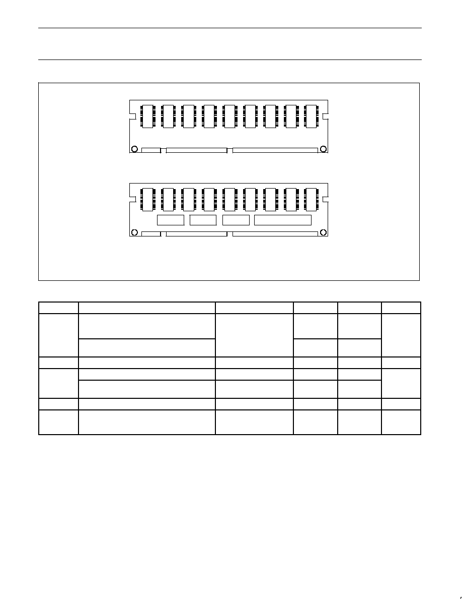
168-pin SDR SDRAM DIMM
SDRAM
SDRAM
SDRAM
SDRAM
SDRAM
SDRAM
SDRAM
SDRAM
SDRAM
The PLL clock distribution device and AVC registered drivers reduce
signal loads on the memory controller and prevent timing delays and
waveform distortions that would cause unreliable operation
SDRAM
SDRAM
SDRAM
SDRAM
SDRAM
SDRAM
SDRAM
SDRAM
SDRAM
AVC16835
PCK2509S or PCK2510S
AVC16835
BACK SIDE
FRONT SIDE
AVC16835
SW00408
RECOMMENDED OPERATING CONDITIONS
SYMBOL
PARAMETER
CONDITIONS
MIN
MAX
UNIT
V
CC
DC supply voltage
(according to JEDEC Low Voltage Standards)
1.65
2.3
3.0
1.95
2.7
3.6
V
CC
DC supply voltage
(for low voltage applications)
1.2
3.6
V
I
DC Input voltage range
0
3.6
V
DC output voltage range; output 3-State
0
3.6
V
O
DC output voltage range;
output HIGH or LOW state
0
V
CC
V
T
amb
Operating free-air temperature range
≠40
+85
∞
C
t
r
, t
f
Input rise and fall times
V
CC
= 1.65 to 2.3 V
V
CC
= 2.3 to 3.0 V
V
CC
= 3.0 to 3.6 V
0
0
0
30
20
10
ns/V
Philips Semiconductors
Preliminary specification
74AVC16835
18-bit Registered Driver (3-State)
1999 Jul 23
5
ABSOLUTE MAXIMUM RATINGS
In accordance with the Absolute Maximum Rating System (IEC 134)
Voltages are referenced to GND (ground = 0V)
SYMBOL
PARAMETER
CONDITIONS
RATING
UNIT
V
CC
DC supply voltage
≠0.5 to +4.6
V
I
IK
DC input diode current
V
I
t
0
≠50
mA
V
I
DC input voltage
For all inputs
1
≠0.5 to 4.6
V
I
OK
DC output diode current
V
O
u
V
CC
or V
O
t
0
"
50
mA
V
O
DC output voltage; output 3-State
Note 1
≠0.5 to 4.6
V
V
O
DC output voltage;
output HIGH or LOW state
Note 1
≠0.5 to V
CC
+0.5
V
I
O
DC output source or sink current
V
O
= 0 to V
CC
"
50
mA
I
GND
, I
CC
DC V
CC
or GND current
"
100
mA
T
stg
Storage temperature range
≠65 to +150
∞
C
P
TOT
Power dissipation per package
≠plastic thin-medium-shrink (TSSOP)
For temperature range: ≠40 to +125
∞
C
above +55
∞
C derate linearly with 8 mW/K
600
mW
NOTE:
1. The input and output voltage ratings may be exceeded if the input and output current ratings are observed.
DC ELECTRICAL CHARACTERISTICS
Over recommended operating conditions. Voltage are referenced to GND (ground = 0 V).
LIMITS
SYMBOL
PARAMETER
TEST CONDITIONS
Temp = -40
∞
C to +85
∞
C
UNIT
MIN
TYP
1
MAX
V
CC
= 1.2 V
V
CC
≠
≠
V
IH
HIGH level Input voltage
V
CC
= 1.65 to 1.95 V
0.65V
CC
0.9
≠
V
V
IH
HIGH level In ut voltage
V
CC
= 2.3 to 2.7 V
1.7
1.2
≠
V
V
CC
= 3.0 to 3.6 V
2.0
1.5
≠
V
CC
= 1.2 V
≠
≠
GND
V
IL
LOW level Input voltage
V
CC
= 1.65 to 1.95 V
≠
0.9
0.35V
CC
V
V
IL
LOW level In ut voltage
V
CC
= 2.3 to 2.7 V
≠
1.2
0.7
V
V
CC
= 3.0 to 3.6 V
≠
1.5
0.8
V
CC
= 1.65 to 3.6 V; V
I
= V
IH
or V
IL
;
V
CC
*
0 20
V
CC
≠
CC
I
IH
IL
I
O
= ≠100
µ
A
V
CC
*
0.20
V
CC
≠
V
OH
HIGH level output voltage
V
CC
= 1.65 V; V
I
= V
IH
or V
IL
; I
O
= ≠4 mA
V
CC
*
0.45
V
CC
*
0.10
≠
V
V
CC
= 2.3 V; V
I
= V
IH
or V
IL
; I
O
= ≠8 mA
V
CC
*
0.55
V
CC
*
0.28
≠
V
CC
= 3.0 V; V
I
= V
IH
or V
IL
; I
O
= ≠12 mA
V
CC
*
0.70
V
CC
*
0.32
≠
V
CC
= 1.65 to 3.6 V; V
I
= V
IH
or V
IL
;
≠
GND
0 20
CC
I
IH
IL
I
O
= 100
µ
A
≠
GND
0.20
V
OL
LOW level output voltage
V
CC
= 1.65 V; V
I
= V
IH
or V
IL
; I
O
= 4 mA
≠
0.10
0.45
V
V
CC
= 2.3 V; V
I
= V
IH
or V
IL
; I
O
= 8 mA
≠
0.26
0.55
V
CC
= 3.0 V; V
I
= V
IH
or V
IL
; I
O
= 12 mA
≠
0.36
0.70
V
CC
= 1 65 to 3 6 V;
I
I
Input leakage current
V
CC
= 1.65 to 3.6 V
V
I
= V
CC
or GND
≠
0.1
2.5
µ
A
I
g
V
I
= V
CC
or GND
µ
I
OFF
3-State output OFF-state current
V
CC
= 0 V; V
I
or V
O
= 3.6 V
≠
0.1
"
10
µ
A
I
IHZ
/I
ILZ
3-State output OFF-state current
V
CC
= 1.65 to 3.6 V; V
I
= V
CC
or GND
≠
0.1
12.5
µ
A
I
OZ
3-State output OFF-state current
V
CC
= 1.65 to 2.7 V; V
I
= V
IH
or V
IL
;
V
O
= V
CC
or GND
≠
0.1
5
µ
A
I
OZ
3-State out ut OFF-state current
V
CC
= 3.0 to 3.6 V; V
I
= V
IH
or V
IL
;
V
O
= V
CC
or GND
≠
0.1
10
µ
A
I
CC
Quiescent supply current
V
CC
= 1.65 to 2.7 V; V
I
= V
CC
or GND; I
O
= 0
≠
0.1
20
µ
A
I
CC
Quiescent su
ly current
V
CC
= 3.0 to 3.6 V; V
I
= V
CC
or GND; I
O
= 0
≠
0.2
40
µ
A
NOTES:
1. All typical values are at T
amb
= 25
∞
C.