 | –≠–ª–µ–∫—Ç—Ä–æ–Ω–Ω—ã–π –∫–æ–º–ø–æ–Ω–µ–Ω—Ç: 74HC133 | –°–∫–∞—á–∞—Ç—å:  PDF PDF  ZIP ZIP |
Document Outline
- FEATURES
- GENERAL DESCRIPTION
- ORDERING INFORMATION
- QUICK REFERENCE DATA
- ORDERING INFORMATION
- PINNING
- FUNCTION TABLE
- DC CHARACTERISTICS
- AC CHARACTERISTICS
- PACKAGE OUTLINES
DATA SHEET
Product specification
File under Integrated Circuits, IC06
September 1993
INTEGRATED CIRCUITS
74HC133
13-input NAND gate
For a complete data sheet, please also download:
∑
The IC06 74HC/HCT/HCU/HCMOS Logic Family Specifications
∑
The IC06 74HC/HCT/HCU/HCMOS Logic Package Information
∑
The IC06 74HC/HCT/HCU/HCMOS Logic Package Outlines
September 1993
2
Philips Semiconductors
Product specification
13-input NAND gate
74HC133
FEATURES
∑
Output capability: standard
∑
I
CC
category: SSI
GENERAL DESCRIPTION
The HC133 is an high-speed Si-gate CMOS device and is pin compatible with low power Schottky TTL (LSTTL).
It is specified in compliance with JEDEC standard no. 7A.
The 74HC133 provides the 13-input NAND function.
QUICK REFERENCE DATA
GND = 0 V; T
amb
= 25
∞
C; t
r
= t
f
= 6 ns
Notes to the quick reference data
1. C
PD
is used to determine the dynamic power dissipation (P
D
in
µ
W)
P
D
= C
PD
◊
V
CC
2
◊
f
i
+
(C
L
◊
V
CC
2
◊
f
o
) where:
f
i
= input frequency in MHz; C
L
= output load capacitance in pF;
f
o
= output frequency in MHz; V
CC
= supply voltage in V;
(C
L
◊
V
CC
2
◊
f
o
) = sum of the outputs.
2. For HC the condition is V
I
= GND to V
CC
ORDERING INFORMATION
See also
"74HC/HCT/HCU/HCMOS Logic Package Information"
.
SYMBOL
PARAMETER
CONDITIONS
TYPICAL
UNIT
t
PHL
/t
PLH
propagation delay A..M to Y
C
L
= 15 pF; V
CC
= 5 V
9
ns
C
I
input capacitance
3.5
pF
C
PD
power dissipation per gate
notes 1 and 2
19
pF
TYPE NUMBER
PACKAGES
PINS
PIN POSITION
MATERIAL
CODE
74HC133N
16
DIL
plastic
SOT38
74HC133D
16
SO
plastic
SOT109A
September 1993
3
Philips Semiconductors
Product specification
13-input NAND gate
74HC133
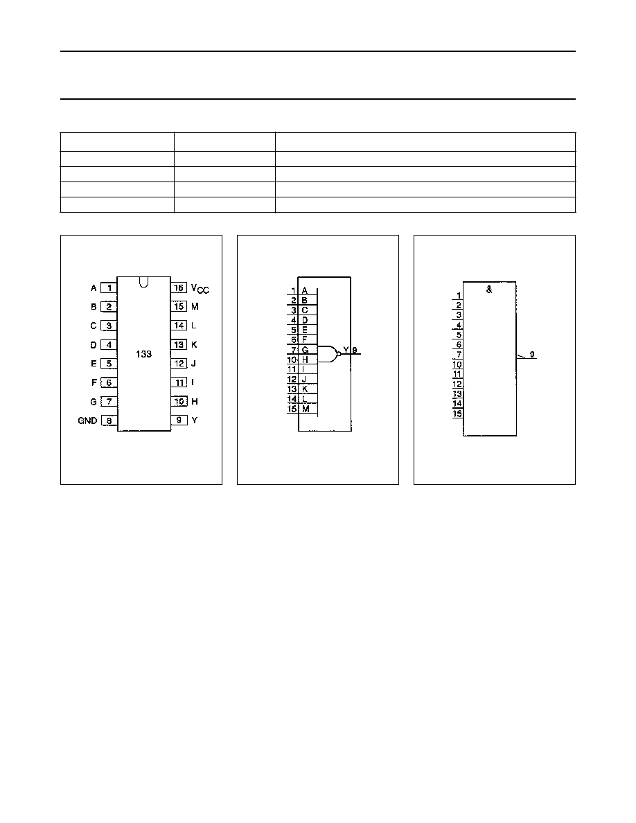
PINNING
PIN NO.
SYMBOL
NAME AND FUNCTION
1..7, 10.. 15
A.. G, H..M
data input
8
GND
ground (0 V)
9
Y
data output
16
V
CC
positive supply voltage
Fig.1 Pin configuration.
Fig.2 Logic symbol.
Fig.3 IEC logic symbol.
September 1993
4
Philips Semiconductors
Product specification
13-input NAND gate
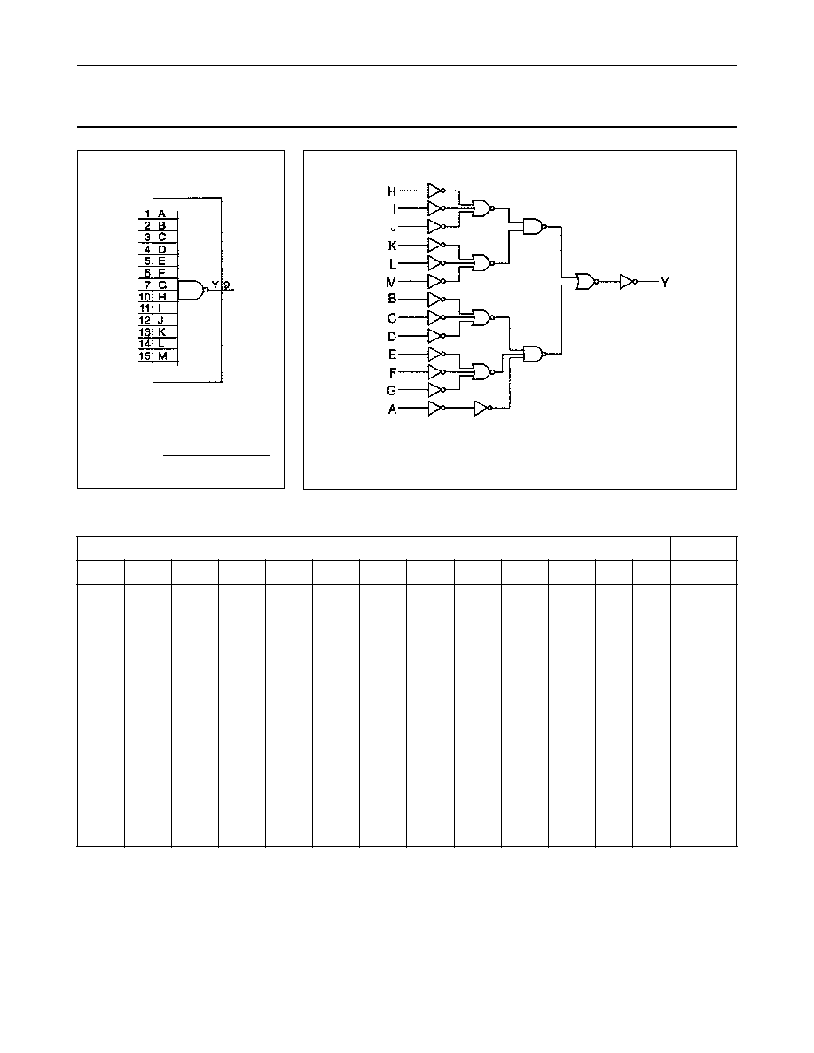
74HC133
Fig.4
Functional diagram;
Y = ABCDEFGHIJKLM.
Fig.5 Logic diagram.
FUNCTION TABLE
Notes
1. H = HIGH voltage level
L = LOW voltage level
X = don't care
INPUTS
OUTPUT
A
B
C
D
E
F
G
H
I
J
K
L
M
Y
L
X
X
X
X
X
L
X
X
X
X
X
L
X
X
X
X
X
L
X
X
X
X
X
L
X
X
X
X
X
X
X
X
X
X
X
X
X
X
X
X
X
X
X
X
X
X
X
X
X
X
X
X
X
X
X
X
X
X
X
X
X
X
X
X
H
H
H
H
H
X
X
X
X
X
X
X
X
X
X
X
X
X
X
X
X
X
X
X
X
X
X
X
X
X
L
X
X
X
X
X
L
X
X
X
X
X
L
X
X
X
X
X
L
X
X
X
X
X
L
X
X
X
X
X
X
X
X
X
X
X
X
X
X
X
H
H
H
H
H
X
X
X
H
X
X
X
H
X
X
X
H
X
X
X
H
X
X
X
H
X
X
X
H
X
X
X
H
X
X
X
H
X
X
X
H
X
X
X
H
L
X
X
H
X
L
X
H
X
X
L
H
H
H
H
L
September 1993
5
Philips Semiconductors
Product specification
13-input NAND gate
74HC133
DC CHARACTERISTICS FOR 74HC
For the DC characteristics see
"74HC/HCT/HCU/HCMOS Logic Family Specifications"
.
Output capability: standard
I
CC
category: SSI
AC CHARACTERISTICS FOR 74HC
GND = 0 V; t
f
= t
r
= 6 ns; C
L
= 50 pF
PACKAGE OUTLINES
See
"74HC/HCT/HCU/HCMOS Logic Package Outlines"
.
SYMBOL
PARAMETER
T
amb
(
∞
C)
TEST CONDITIONS
+25
-
40 to +85
-
40 to +125
UNIT
V
CC
(V)
WAVEFORMS
MIN. TYP.
MAX.
MIN.
MAX.
MIN.
MAX.
t
PHL
/t
PLH
propagation delay
A..M to Y
-
-
-
36
13
10
110
22
19
-
-
-
140
28
23
-
-
-
165
33
28
ns
2.0
4.5
6.0
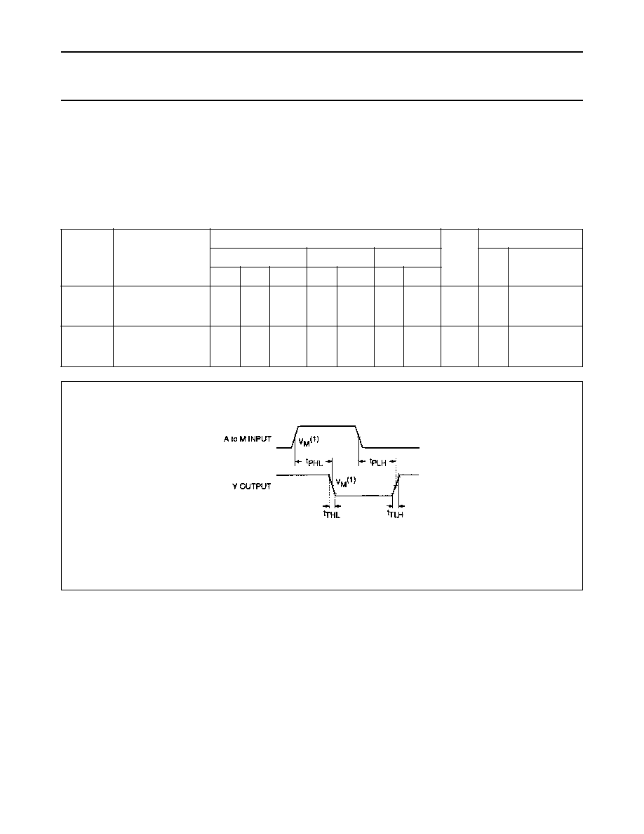
Fig.6
t
THL
/t
TLH
output transition
time
-
-
-
19
7
6
75
15
13
-
-
-
95
19
16
-
-
-
110
22
19
ns
2.0
4.5
6.0
Fig.6
Fig.6
Waveforms showing the input (A, B, C, D, E, F, G, H, I, J, K, L, M) to output (Y) propagation delays and
the output transition times.
(1) HC: V
M
= 50%; V
I
= GND to V
CC
.