DATA SHEET
Product specification
Supersedes data of September 1993
File under Integrated Circuits, IC06
1998 Jun 10
INTEGRATED CIRCUITS
74HC/HCT181
4-bit arithmetic logic unit
For a complete data sheet, please also download:
∑
The IC06 74HC/HCT/HCU/HCMOS Logic Family Specifications
∑
The IC06 74HC/HCT/HCU/HCMOS Logic Package Information
∑
The IC06 74HC/HCT/HCU/HCMOS Logic Package Outlines

1998 Jun 10
2
Philips Semiconductors
Product specification
4-bit arithmetic logic unit
74HC/HCT181
FEATURES
∑
Full carry look-ahead for high-speed arithmetic
operation on long words
∑
Provides 16 arithmetic operations: add, subtract,
compare, double, plus 12 others
∑
Provides all 16 logic operations of two variables:
EXCLUSIVE-OR, compare, AND, NAND, NOR, OR plus
10 other logic operations
∑
Output capability:
standard,
A=B open drain
∑
I
CC
category: MSI
GENERAL DESCRIPTION
The 74HC/HCT181 are high-speed Si-gate CMOS devices
and are pin compatible with low power Schottky TTL
(LSTTL). They are specified in compliance with JEDEC
standard no. 7A.
The 74HC/HCT181 are 4-bit high-speed parallel
Arithmetic Logic Units (ALU). Controlled by the four
function select inputs (S
0
to S
3
) and the mode control input
(M), they can perform all the 16 possible logic operations
or 16 different arithmetic operations on active HIGH or
active LOW operands (see function table).
When the mode control input (M) is HIGH, all internal
carries are inhibited and the device3 performs logic
operations on the individual bits as listed. When M is LOW,
the carries are enabled and the "181" performs arithmetic
operations on the two 4-bit words. The "181" incorporates
full internal carry look-ahead and provides for either ripple
carry between devices using the C
n+4
output, or for carry
look-ahead between packages using the carry
propagation (P) and carry generate (G) signals. P and
G are not affected by carry in.
When speed requirements are not stringent, it can be used
in a simple ripple carry mode by connecting the carry
output (C
n+4
) signal to the carry input (C
n
) of the next unit.
For high-speed operation the device is used in conjunction
with the "182" carry look-ahead circuit. One carry
look-ahead package is required for each group of four
"181" devices. Carry look-ahead can be provided at
various levels and offers high-speed capability over
extremely long word lengths.
The comparator output (A=B) of the device goes HIGH
when all four function outputs (F
0
to F
3
) are HIGH and can
be used to indicate logic equivalence over 4 bits when the
unit is in the subtract mode. A=B is an open collector
output and can be wired-AND with other A=B outputs to
give a comparison for more than 4 bits. The open drain
output A=B should be used with an external pull-up
resistor in order to establish a logic HIGH level. The A=B
signal can also be used with the C
n+4
signal to indicate
A
>
B and A
<
B.
The function table lists the arithmetic operations that are
performed without a carry in. An incoming carry adds a one
to each operation. Thus, select code LHHL generates
A minus B minus 1 (2s complement notation) without a
carry in and generates A minus B when a carry is applied.
Because subtraction is actually performed by
complementary addition (1s complement), a carry out
means borrow; thus, a carry is generated when there is no
under-flow and no carry is generated when there is
underflow.
As indicated, the "181" can be used with either active LOW
inputs producing active LOW outputs or with active HIGH
inputs producing active HIGH outputs.
For either case the table lists the operations that are
performed to the operands.
ORDERING INFORMATION
TYPE
NUMBER
PACKAGE
NAME
DESCRIPTION
VERSION
74HC181N3;
74HCT181N3
DIP24
plastic dual in-line package; 24 leads (300 mil)
SOT222-1
74HC181N;
74HCT181N
DIP24
plastic dual in-line package; 24 leads (600 mil)
SOT101-1
74HC181D;
74HCT181D
SO24
plastic small outline package; 24 leads; body width 7.5 mm
SOT137-1
1998 Jun 10
3
Philips Semiconductors
Product specification
4-bit arithmetic logic unit
74HC/HCT181
QUICK REFERENCE DATA
GND = 0 V; T
amb
= 25
∞
C; t
r
= t
f
= 6 ns
Notes
1. C
PD
is used to determine the dynamic power dissipation (P
D
in
µ
W):
P
D
= C
PD
◊
V
CC
2
◊
f
i
+
(C
L
◊
V
CC
2
◊
f
o
) where:
f
i
= input frequency in MHz
f
o
= output frequency in MHz
(C
L
◊
V
CC
2
◊
f
o
) = sum of outputs
C
L
= output load capacitance in pF
V
CC
= supply voltage in V
2. For HC the condition is V
I
= GND to V
CC
For HCT the condition is V
I
= GND to V
CC
-
1.5 V
SYMBOL
PARAMETER
CONDITIONS
TYPICAL
UNIT
HC
HCT
t
PHL
/ t
PLH
propagation delay
C
L
= 15 pF; V
CC
= 5 V
A
n
or B
n
to A=B
28
30
ns
C
n
to C
n+
4
17
21
ns
C
I
input capacitance
3.5
3.5
pF
C
PD
power dissipation capacitance
per L package
notes 1 and 2
90
92
pF
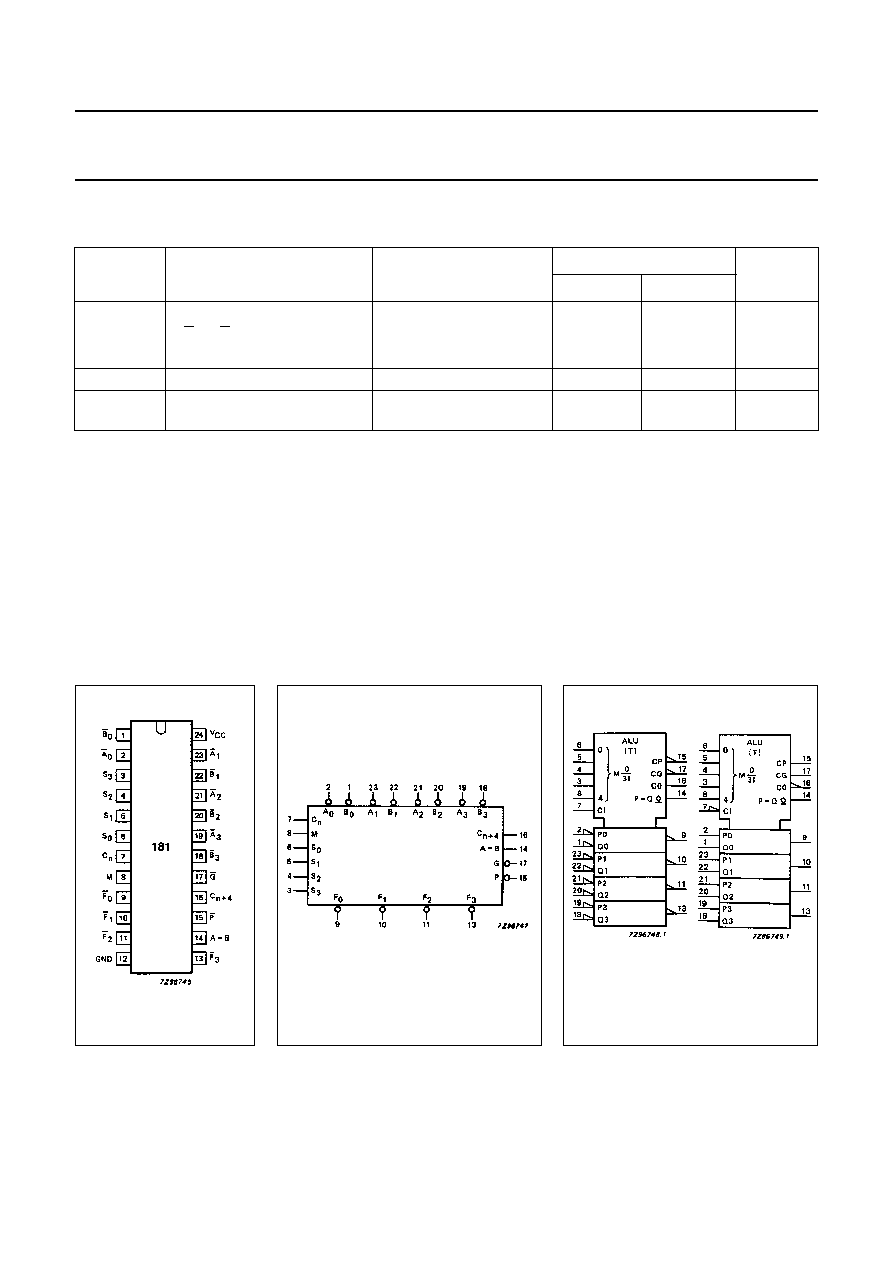
Fig.1 Pin configuration.
Fig.2 Logic symbol.
Fig.3 IEC logic symbol.
A
B
1998 Jun 10
4
Philips Semiconductors
Product specification
4-bit arithmetic logic unit
74HC/HCT181
PIN DESCRIPTION
PIN NO.
SYMBOL
NAME AND FUNCTION
1, 22, 20, 18
B
0
to B
3
operand inputs (active LOW)
2, 23, 21, 19
A
0
to A
3
operand inputs (active LOW)
6, 5, 4, 3
S
0
to S
3
select inputs
7
C
n
carry input
8
M
mode control input
9, 10, 11, 13
F
0
to F
3
function outputs (active LOW)
12
GND
ground (0 V)
14
A=B
comparator output
15
P
carry propagate output (active LOW)
16
C
n+4
carry output
17
G
carry generate output (active LOW)
24
V
CC
positive supply voltage
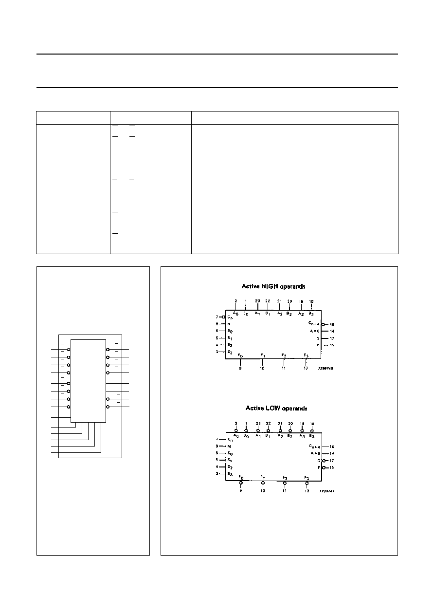
Fig.4 Functional diagram.
ok, halfpage
MBK219
A0
A1
A2
2
23
21
19
1
22
20
18
15
17
14
16
13
11
10
9
A3
B0
B1
Cn
+
4
F3
F2
F1
F0
A=B
G
B2
P
B3
7
Cn
6
S0
5
S1
4
S2
3
S3
8
M
Fig.5 Active HIGH operands - active LOW operands.
1998 Jun 10
5
Philips Semiconductors
Product specification
4-bit arithmetic logic unit
74HC/HCT181
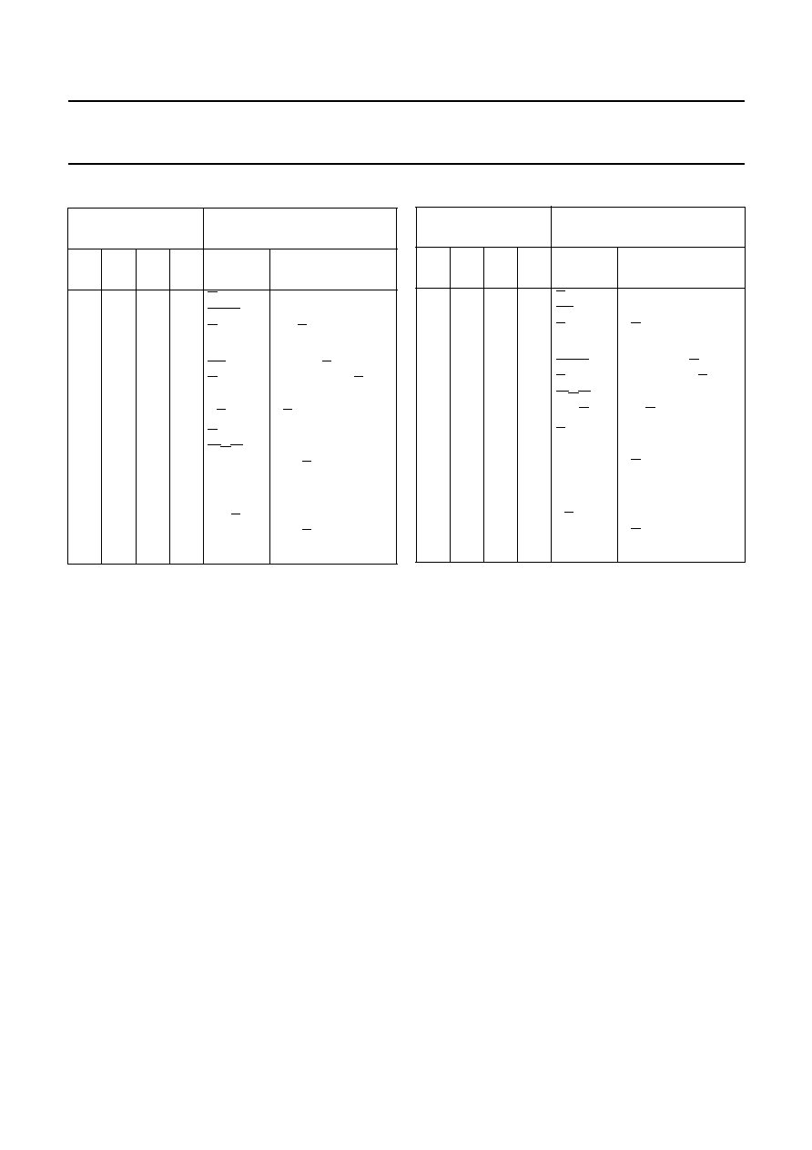
FUNCTION TABLES
Notes to the function tables
1. Each bit is shifted to the next more significant position.
2. Arithmetic operations expressed in 2s complement
notation.
H = HIGH voltage level
L = LOW voltage level
MODE SELECT
INPUTS
ACTIVE HIGH INPUTS AND
OUTPUTS
S
3
S
2
S
1
S
0
LOGIC
(M=H)
ARITHMETIC
(2)
(M=L; C
n
=H)
L
L
L
L
L
L
L
L
L
L
H
H
L
H
L
H
A
A + B
AB
logical 0
A
A + B
A + B
minus 1
L
L
L
L
H
H
H
H
L
L
H
H
L
H
L
H
AB
B
A
B
AB
A plus AB
(A + B) plus AB
A minus B minus 1
AB minus 1
H
H
H
H
L
L
L
L
L
L
H
H
L
H
L
H
A + B
A
B
B
AB
A plus AB
A plus B
(A + B) plus AB
AB minus 1
H
H
H
H
H
H
H
H
L
L
H
H
L
H
L
H
logical 1
A + B
A + B
A
A plus A
(1)
(A + B) plus A
(A + B) plus A
A minus 1
Notes to the function tables
1. Each bit is shifted to the next more significant position.
2. Arithmetic operations expressed in 2s complement
notation.
H = HIGH voltage level
L = LOW voltage level
MODE SELECT
INPUTS
ACTIVE LOW INPUTS AND
OUTPUTS
S
3
S
2
S
1
S
0
LOGIC
(M=H)
ARITHMETIC
(2)
(M=L; C
n
=L)
L
L
L
L
L
L
L
L
L
L
H
H
L
H
L
H
A
AB
A + B
logical 1
A minus 1
AB minus 1
AB minus 1
minus 1
L
L
L
L
H
H
H
H
L
L
H
H
L
H
L
H
A + B
B
A
B
A + B
A plus (A + B)
AB plus (A + B)
A minus B minus 1
A + B
H
H
H
H
L
L
L
L
L
L
H
H
L
H
L
H
AB
A
B
B
A + B
A plus (A + B)
A plus B
AB plus (A + B)
A + B
H
H
H
H
H
H
H
H
L
L
H
H
L
H
L
H
logical 0
AB
AB
A
A plus A
(1)
AB plus A
AB plus A
A